Finfet vs Mosfet: What are Differences
 Published: Mar 01, 2024
Contents
FinFET and MOSFET, two integral components in semiconductor technology, embody distinct approaches to transistor design. FinFET, with its innovative three-dimensional structure, has emerged as a transformative technology, promising improved efficiency and performance. Meanwhile, MOSFET, with its well-established planar structure, remains a stalwart in electronic applications. This comprehensive exploration delves into the structures, functionalities, advantages, disadvantages, and future trends of FinFET and MOSFET, providing insights into the dynamic landscape of semiconductor devices.
What is Finfet
A FinFET, short for Fin Field-Effect Transistor, represents an innovative type of semiconductor transistor, specifically a complementary metal-oxide-semiconductor (CMOS) transistor. It departs from traditional planar transistor structures by introducing a unique 3D design with a fin-shaped channel. This fin-like structure allows for enhanced control over the flow of current.
In contrast to standard transistors where the gate influences current on only one side, FinFET's gate features a three-dimensional, fork-shaped design, enabling control on both sides of the channel. This architectural advancement improves circuit control, minimizes leakage current, and significantly reduces the gate length of the transistor.
FinFET technology has become integral in various electronic devices, including home computers, laptops, tablets, smartphones, wearables, high-end networks, and automotive applications. Its 3D structure and superior control over current flow make it a pivotal component for achieving improved performance, energy efficiency, and scalability in semiconductor technology.
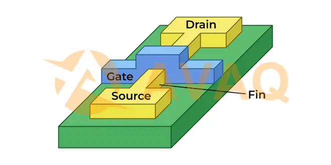
Finfet Structure
FinFET is a three-dimensional transistor structure characterized by vertically arranged fins. Its basic configuration includes the Fin (fin), Gate (gate), Drain (drain), Source (source), and Substrate. The Fin serves as the channel, the Gate controls the flow of electric current, while the Drain and Source play roles akin to traditional MOSFETs, managing the input and output of current. The Substrate acts as the foundation for the entire structure, aiding in device isolation within the chip. FinFET's distinctive design enhances current control, providing superior performance in semiconductor technology.
How Does Finfet Work?
A FinFET is a type of transistor that operates similarly to a traditional MOS transistor but with a unique 3D structure. The name "FinFET" comes from its fin-shaped design. In a FinFET, the transistor structure is folded along the gate length, allowing the gate to control the conducting channel on both sides of the fin. This feature enhances conduction efficiency.
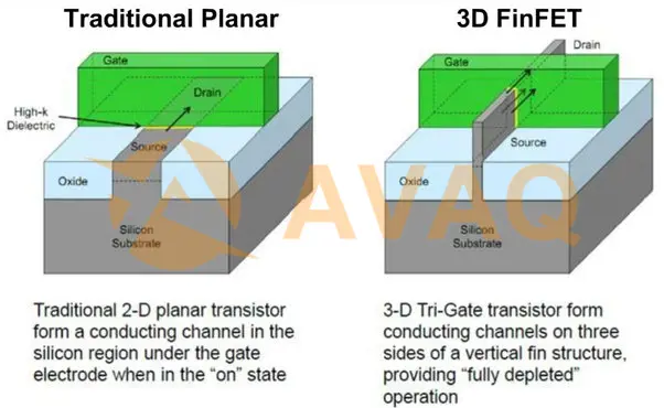
To visualize a FinFET, imagine folding a square piece of paper to create a tent-like structure, representing the gate and oxide. This folded structure is filled with silicon, and folded source and drain contacts are added on either side, forming the fin. This 3D design improves the transistor's performance, and its representation on paper involves a cross-section in the x-z plane, differing from the planar MOSFET.
In summary, a FinFET's distinctive 3D structure enhances conduction control, making it a more efficient and high-performance transistor.
Advantages and Disadvanatages of Finfet
Advantages of FinFET:
Better Control over the Channel:
FinFETs provide improved control over the channel due to their 3D fin-shaped structure, allowing for more effective regulation of current flow.
Suppressed Short-Channel Effects:
The unique design of FinFETs helps mitigate short-channel effects, enhancing the transistor's performance and reliability.
Lower Static Leakage Current:
FinFETs exhibit reduced static leakage current, contributing to enhanced energy efficiency and lower power consumption.
Faster Switching Speed:
The 3D architecture of FinFETs enables faster switching speeds, improving overall transistor performance.
Higher Drain Current (More Drive-Current per Footprint):
FinFETs offer a higher drain current, allowing for increased drive-current per unit area, which is beneficial for high-performance applications.
Lower Switching Voltage:
FinFETs typically operate at lower switching voltages, reducing power requirements and contributing to energy efficiency.
Low Power Consumption:
The combination of lower static leakage current and efficient switching contributes to overall lower power consumption in FinFET-based devices.
Disadvantages of FinFET:
Difficult to Control Dynamic Vth:
Dynamic threshold voltage (Vth) control can be challenging in FinFETs, posing complexities in certain operational scenarios.
Quantized Device-Width:
FinFETs have a quantized device-width, making it impossible to specify dimensions in fractions of fins. Designers must adhere to multiples of whole fins.
Higher Parasitics Due to 3-D Profile:
The 3D profile of FinFETs introduces higher parasitic capacitances and resistances, potentially impacting overall performance.
Very High Capacitances:
FinFETs can exhibit very high capacitances, affecting their ability to maintain low power consumption in certain applications.
Corner Effect:
The corner effect in FinFETs results in an amplified electric field at the corners compared to the sidewalls, which can be mitigated using specific design techniques such as nitrate layers.
High Fabrication Cost:
The complex 3D structure and additional fabrication steps contribute to higher manufacturing costs for FinFETs compared to traditional transistor technologies.
In conclusion, while FinFETs offer several advantages, including improved control and lower power consumption, they come with challenges such as quantized dimensions and higher parasitics, making careful consideration necessary in their application and design.
What is Mosfet
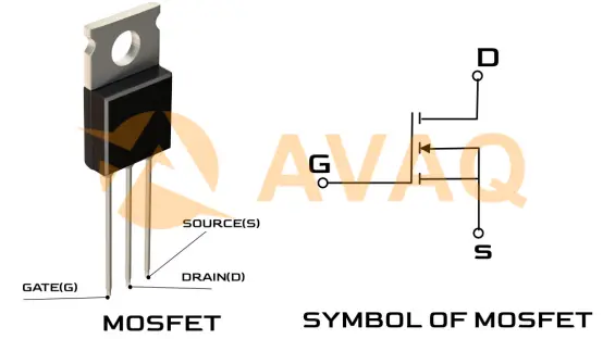
A Metal-Oxide-Semiconductor Field-Effect Transistor (MOSFET, MOS-FET, or MOS FET) represents a type of field-effect transistor (FET) featuring an insulated gate, where voltage governs the device's conductivity. Primarily employed for signal switching and amplification, its capability to alter conductivity based on applied voltage is instrumental in electronic signal modulation.
In MOSFETs, silicon dioxide constitutes the gate, providing isolation by impeding direct charge flow from the gate to the conducting channel. This insulation is pivotal in the MOSFET's role as a voltage-controlled device.
Notably, MOSFETs have surpassed Bipolar Junction Transistors (BJTs) in prevalence within both digital and analog circuits. The abundance of MOSFETs in digital applications, such as memory chips and microprocessors, underscores their significance. Their versatility extends to complementary metal-oxide-semiconductor (CMOS) logic, where pairs of MOS transistors, fabricated with either p-type or n-type semiconductors, facilitate switching circuits characterized by exceptionally low power consumption.
The dominance of MOSFETs in digital circuits, owing to their scalability, efficiency, and low power requirements, underscores their indispensable role in modern electronics.
Mosfet Structure
MOSFETs, or Metal-Oxide-Semiconductor Field-Effect Transistors, exhibit a planar structure characterized by the integration of metal, oxide, and semiconductors. In the case of a planar n-channel MOSFET, the transistor is created by diffusing heavily doped n-type regions onto a p-substrate body. Atop this planar configuration, a layer of silicon dioxide is cultivated. Metallic terminals are selectively etched onto the insulating layer of silicon dioxide. The metallic terminals that establish contact with the n-type regions beneath assume the roles of drain and source. The gate terminal, positioned on the silicon dioxide layer without contact with the n-type regions, completes the basic structure of the planar MOSFET.
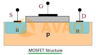
The MOSFET is a four-terminal device with Source (S), Drain (D), Gate (G), and body (B) terminals. Often, the body (B) is connected to the source terminal, reducing the terminals to three. Its operation involves adjusting the width of a channel through which charge carriers (electrons or holes) flow.
Charge carriers enter the channel at the source and exit through the drain. The channel width is regulated by the voltage applied to the Gate electrode, positioned between the source and drain. This Gate is insulated from the channel by an extremely thin layer of metal oxide.
The MOSFET is alternatively referred to as a metal-insulator-semiconductor field-effect transistor (MISFET) or an insulated-gate field-effect transistor (IGFET).
Working Principle of Mosfet
The operational principle of a MOSFET hinges on the behavior of the MOS capacitor, a crucial component of the MOSFET structure. The semiconductor surface beneath the oxide layer, positioned between the source and drain terminals, plays a pivotal role and can transition from p-type to n-type based on applied gate voltages.
Upon the application of a positive gate voltage, holes beneath the oxide layer encounter a repulsive force, prompting their downward movement into the substrate. Simultaneously, the depletion region accumulates bound negative charges linked to acceptor atoms. Electrons migrate towards this region, forming a channel. The positive gate voltage also attracts electrons from the n+ source and drain regions into the channel.
Subsequently, if a voltage is introduced between the drain and source, current can flow freely between these terminals, and the gate voltage governs the behavior of electrons within the channel. Conversely, the application of a negative voltage results in the formation of a hole channel beneath the oxide layer. This dynamic interplay enables the MOSFET to regulate the flow of current based on the applied gate voltage, making it a versatile and controlled semiconductor device.
Advantages and Disadvanatages of Mosfet
Advantages:
- Scalability: MOSFETs exhibit exceptional scalability, allowing for downsizing in dimensions. This characteristic facilitates increased component integration on the chip surface, a crucial feature in modern electronic devices.
- Low Power Consumption: MOSFETs are known for their low power consumption, enabling the efficient incorporation of numerous components on a chip, contributing to energy-efficient electronic systems.
- No Gate Diode: Unlike certain transistors, MOSFETs lack a gate diode. This unique feature allows them to operate seamlessly with both positive and negative gate voltages, enhancing their versatility in circuit design.
- Direct Readability: MOSFETs offer direct readability with a very thin active area, streamlining their use in electronic applications where compact design and precision are essential.
- High Drain Resistance: With higher drain resistance due to the lower resistance of the channel, MOSFETs contribute to improved signal control and integrity in electronic circuits.
- Compact Physical Size: In packaged form, MOSFETs possess a physical size of less than 4 mm^2, allowing for the creation of smaller, space-efficient electronic devices.
- Widespread Usage: MOSFETs find extensive applications in VLSI circuits, CMOS digital circuits, microprocessors, and memory devices, underlining their significance in modern electronics.
- Enhancement Type for Digital Circuitry: The prevalence of enhancement-type MOSFETs in digital circuitry underscores their role in advancing digital technology.
- High-Speed Operation: MOSFETs support high-speed operation, making them suitable for applications where rapid switching is essential, such as in digital signal processing.
- High Input Impedance: With high input impedance, MOSFETs offer enhanced signal reception capabilities, making them versatile in various electronic circuits.
- Ease of Fabrication: Fabricating MOSFETs is comparatively easier than certain transistor types, contributing to their widespread adoption in electronic manufacturing.
- Manufacturing Convenience: MOSFETs are easy to manufacture, further contributing to their popularity in the semiconductor industry.
Disadvantages:
- Limited Lifespan: MOSFETs have a finite lifespan, which may pose challenges in applications requiring prolonged device longevity.
- Calibration Requirements: In certain applications, MOSFETs may require repeated calibration for accurate dose measurements, adding complexity to their implementation.
- Susceptibility to Overload Voltage: MOSFETs are highly susceptible to overload voltage, necessitating special handling during installation to prevent potential damage and ensure reliable operation.
Finfet vs Mosfet: What are Differences
|
Aspect |
MOSFET |
FinFET |
|
Structure |
Planar structure |
Three-dimensional or "fin" structure |
|
Gate Control |
Voltage-controlled conductivity |
Voltage-controlled gate width |
|
Leakage Current |
Relatively higher leakage current |
Lower leakage current |
|
Power Efficiency |
Relatively lower power efficiency |
Improved power efficiency |
|
Speed and Performance |
Moderate speed |
Faster switching speed |
|
Transistor Capacitance |
Higher transistor capacitance |
Reduced transistor capacitance |
|
Scalability |
Limited scalability in smaller nodes |
Better scalability in smaller nodes |
|
Integration |
Limited integration capability |
Improved integration capability |
|
Manufacturing Process |
Relatively simpler manufacturing process |
More complex manufacturing process |
|
Cost |
Lower manufacturing cost |
Higher manufacturing cost |
|
Applications |
Wide range of applications |
Similar range of applications as MOSFET |
|
Future Trends |
Limited potential for future improvements |
Further potential for development |
In summary, FinFET and MOSFET are two transistor technologies with distinct characteristics and applications. While MOSFET offers well-established performance and scalability, FinFET brings enhanced power efficiency and improved control over leakage current. Both technologies contribute to the continued advancement of the semiconductor industry and enable innovative electronic devices and systems.
Finfet vs Mosfet: Which is Better
The advent of FinFET technology has introduced significant advantages over traditional MOSFETs, primarily attributed to its three-dimensional structure. These desirable characteristics of FinFETs include:
Higher Integration Density: FinFET technology allows for the incorporation of a large number of transistors on a single chip, making it highly suitable for IC fabrication. This scalability advantage surpasses that of MOSFETs within a given footprint area.
Improved Short-Channel Behavior: As chips shrink in size, MOSFETs face challenges related to short-channel effects. The three-dimensional structure of FinFETs, with fins providing better short-channel behavior, addresses this issue effectively.
Elimination of Channel Doping Fluctuations: In planar MOSFETs, channel doping is common to improve short-channel behavior. However, FinFETs, with their wrap-around gate over a thin body, make channel doping optional, eliminating dopant-induced fluctuations.
Reduced Leakage Current and Power Consumption: FinFETs demonstrate reduced leakage current and voltage, contributing to lower power consumption compared to MOSFETs. The gate wrapping around the drain-source channel minimizes leakage current when the gate is not energized.
Enhanced Drive Strength and Current: FinFETs provide flexibility in increasing drive strength by incorporating multiple or longer fins, in contrast to planar MOSFETs, where drive strength depends on channel width.
Fast Switching Times: The higher drive current in FinFETs translates to faster switching times, making them high-speed devices compared to planar MOSFETs.
Ease of Fabrication for Multi-Gate Devices: Fabricating multi-gate devices is more straightforward with FinFET technology, while it poses challenges in planar MOSFETs.
Superior Subthreshold Slope and Voltage Gain: FinFETs exhibit excellent subthreshold slope and higher voltage gain compared to planar MOSFETs, enhancing their overall performance.
In the FinFET vs. MOSFET comparison, understanding the distinctive advantages of FinFETs underscores their appeal in contemporary semiconductor technology. The low leakage current, improved heat dissipation, reduced DIBL, and consistent threshold voltage make FinFETs a compelling choice for applications demanding advanced performance. Manufacturers have demonstrated the scalability of FinFET technology, showcasing its continued relevance in the evolution of semiconductor manufacturing.
Future Trends for FinFET and MOSFET
In the realm of transistor technology, the future holds promising advancements for both FinFET and MOSFET. For FinFET, ongoing research and development efforts focus on refining its three-dimensional structure, optimizing manufacturing processes, and exploring higher levels of transistor integration on a single chip. These trends aim to further enhance FinFET's scalability, efficiency, and cost-effectiveness, solidifying its role in the semiconductor landscape.
Simultaneously, MOSFETs are expected to evolve by persisting in scaling down to smaller process nodes and exploring hybrid integration with emerging technologies. As researchers delve into alternative transistor structures, including nanowire transistors and 2D materials, the future may witness the emergence of new transistor technologies beyond FinFET. Moreover, innovations in design and materials are anticipated to contribute to improved power efficiency and overall performance for both FinFET and MOSFET.
The integration of traditional transistors with emerging technologies, such as neuromorphic computing and quantum devices, could further shape the landscape. Additionally, customization for specific applications, such as AI, IoT, and edge computing, is likely to drive tailored solutions, ensuring that FinFET and MOSFET technologies continue to play pivotal roles in the ever-evolving field of semiconductor technology.
Conclusion
In the ever-evolving realm of semiconductor technology, FinFET and MOSFET stand as pillars, each contributing unique strengths to the field. While MOSFET showcases reliability, scalability, and versatility, FinFET introduces a paradigm shift with its three-dimensional prowess, promising enhanced efficiency and control. As research propels these technologies forward, the future holds promises of improved integration, scalability, and performance. Whether it be the refined structures of FinFET or the enduring legacy of MOSFET, both technologies continue to shape the landscape of modern electronics, paving the way for innovative applications and advancements.
Next Industry Focus
Xilinx XCF32PVOG48C: Your Complete Buying and Usage Guide with Datasheet
 Update Time: Mar 06, 2024 Consumer Electronics
 FAQ
FAQ
- Are FinFETs more expensive to manufacture than traditional MOSFETs?
- The manufacturing process for FinFETs can be more complex, which may contribute to higher manufacturing costs. However, the benefits in terms of performance and energy efficiency often justify the use of FinFET technology, especially in advanced semiconductor nodes.
- Are FinFETs the latest transistor technology, or are there newer developments?
- FinFETs represent a significant advancement in transistor technology, especially in the transition to smaller semiconductor process nodes. However, ongoing research and development in the field may lead to new transistor technologies in the future.
- Does the adoption of FinFET technology impact device performance?
- Yes, the adoption of FinFET technology has a significant impact on device performance. It allows for the development of more powerful and energy-efficient integrated circuits, enabling the continued advancement of electronic devices.
- In what applications are FinFETs commonly used?
- FinFET technology is widely used in modern semiconductor manufacturing processes, especially in applications requiring high-performance and low-power consumption, such as in processors for computers, mobile devices, and other advanced electronics.
- What are the advantages of FinFET over traditional MOSFETs?
- FinFETs offer several advantages, including improved performance, lower power consumption, and better scalability to smaller process nodes. They are particularly well-suited for advanced semiconductor technologies where traditional planar MOSFETs face challenges.
- How does the three-dimensional fin structure in FinFETs improve performance?
- The fin structure provides better electrostatic control over the channel, allowing more effective modulation of the transistor's conductivity. This improved control results in lower leakage currents, reduced power consumption, and better performance at smaller process nodes.
Related Industry Focus
-
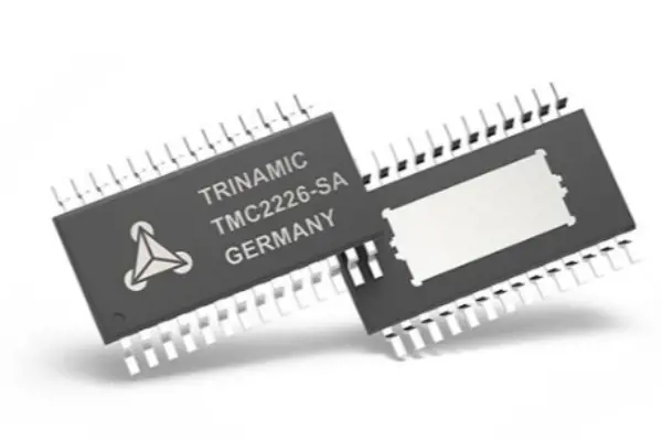
TMC2226 vs TMC2209: What are Differences
The TMC2226 and TMC2209 are advanced motor driver ICs for two-phase stepper motors. Both offer silent operation, precise motion control, and protective features, but the TMC2226 emphasizes noise-free functionality and optimized efficiency, while the TMC2209 focuses on c...
Published: 2023-12-08 17:49:40 -

RC4558 Op Amp: Datasheet PDF, Pinout Features and Equivalent
The RC4558 is a dual general-purpose operational amplifier known for its versatility in various applications. It shares similarities with the LM741 but lacks the offset null capability. This amplifier offers a high common-mode input voltage range, suitable for voltage-f...
Published: 2023-12-06 18:08:42 -
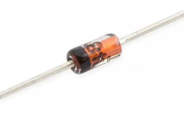
1N914 vs 1N4148: What are Differences and How to Choose
This article aims to dissect the distinctions between these diodes, explore their specifications, and provide insights into the factors that guide the selection between the J1N914 and 1N4148 diodes for diverse electronic applications.
Published: 2023-12-05 17:55:26 -
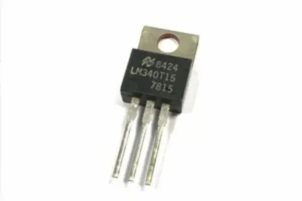
IC 7815 Voltage Regulator: Pinout, Datasheet and How to Use
The IC 7815 is a fixed-voltage integrated circuit voltage regulator commonly used in electronic circuits to maintain a constant output voltage despite fluctuations in the input voltage.
Published: 2023-12-01 18:16:10
 Popular Industry Focus
Hot Products
-
MCP4231-502E/P
Microchip Technology, Inc
Digital Potentiometer 5k Ohm 2 Circuit 129 Taps SPI Interface 14-PDIP
-
JANTX1N5283-1
Microchip Technology, Inc
Current Regulator Diodes Current Regulators
-
COM20022I-HT
Microchip Technology, Inc
ARCNET Controller ARCNET 878.1 Parallel Interface 48-TQFP (7x7)
-
SY88903ALKGTR
Microchip Technology, Inc
Limiting Postamplifier IC Optical Networks 10-MSOP
-
LPC47N350-NU
Microchip Technology, Inc
I/O Controller Interface IC Advanced I/O Controller
-
HV9911NG-G-M934
Microchip Technology, Inc
Switch-Mode LED Driver IC w/ High Current Accuracy.
Related Parts
-
FP75R07N2E4BOSA1
Infineon Technologies Corporation
IGBT MODULE 650V 95A
-

MMUN2233LT1G
ON Semiconductor, LLC
NPN Bipolar Digital Transistor (BRT)
-

FP50R12N2T7PBPSA1
Infineon Technologies Corporation
IGBT Module Trench Field Stop Three Phase Inverter 1200 V 50 A 20 mW Chassis Mount AG-ECONO2B
-
IRF6795MTRPBF
Infineon Technologies Corporation
MOSFET 25V 1 N-CH HEXFET 1.8mOhms 35nC
-
EMF17T2R
ROHM Semiconductor
Bipolar Transistors - Pre-Biased DUAL PNP/DTR
-
MRF10005
MACOM Technology Solutions
RF Bipolar Transistors Transistor,960-1215Mhz,28V,5W
-
IRFZ46NPBF
Infineon Technologies Corporation
N-Channel 55 V 53A (Tc) 107W (Tc) Through Hole TO-220AB
-
SMUN5211DW1T1G
ON Semiconductor, LLC
Pre-Biased Bipolar Transistor (BJT) 2 NPN - Pre-Biased (Dual) 50V 100mA 187mW Surface Mount SC-88/SC70-6/SOT-363
-
DTC144EKAT146
ROHM Semiconductor
Trans Digital BJT NPN 50V 100mA 3-Pin SMT T/R
-
MRFE6VP5300GNR1
NXP Semiconductor
RF Mosfet 50 V 100 mA 1.8MHz ~ 600MHz 27dB 300W TO-270 WB-4 Gull
-
FF450R06ME3BOSA1
Infineon Technologies Corporation
IGBT Module Trench Field Stop 2 Independent 600 V 550 A 1250 W Chassis Mount Module
-
FS50R07W1E3B11ABOMA1
Infineon Technologies Corporation
IGBT Modules EASY PACK
-
ULN2003BDR
Texas Instruments, Inc
50-V, 7-ch darlington array with 3-V input capability and low cost
-
FZ600R12KP4
Infineon Technologies Corporation
IGBT Modules IGBT 1200V 600A
-
IRFP7430PBF
Infineon Technologies Corporation
MOSFET 40V 195A 1.4mOhm HEXFET 366W 300nC
Featured Manufacturers