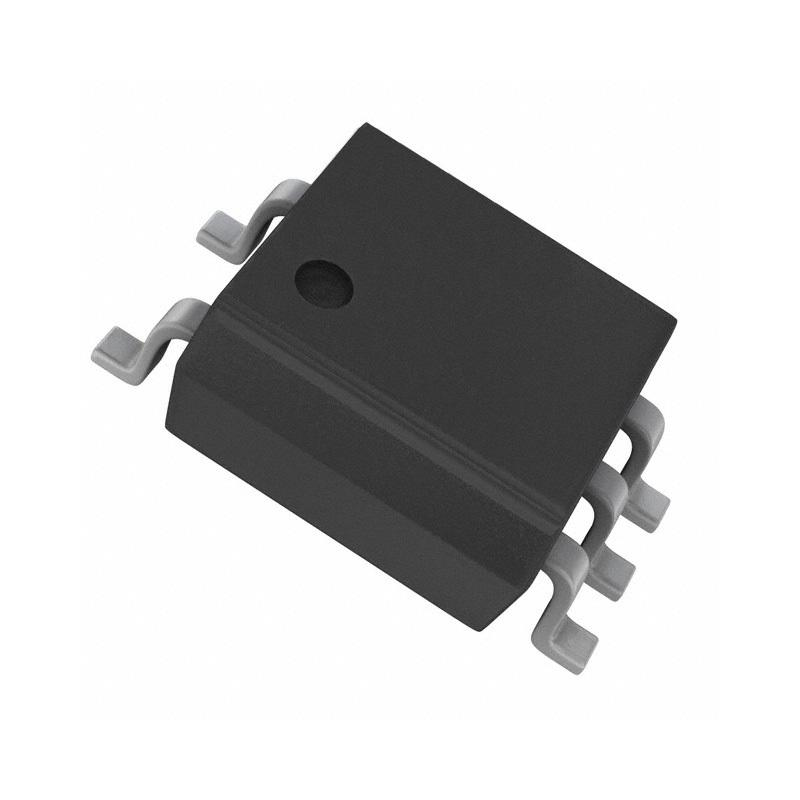
PT2399 IC Delay Echo Audio Processor: Datasheet, Pinout and Application
 Published: Nov 27, 2023
Contents
Introduction to PT2399 IC
The PT2399 is a versatile CMOS single-chip echo processor integrated circuit, renowned for its functionality in creating delay effects. This digital chip incorporates an ADC (Analog-to-Digital Converter) that seamlessly converts incoming analog audio signals into a binary bitstream. Subsequently, this data is stored within an internal 44Kbit RAM for processing. Upon processing, the DAC (Digital-to-Analog Converter) and a low-pass filter decode the bitstream, enabling the transformation of the processed signal.

An inherent feature of the PT2399 lies in its internal VCO (Voltage-Controlled Oscillator) clock frequency, which fundamentally determines the duration of the overall delay effect. This distinctive aspect grants users the flexibility to easily modify the VCO frequency by adjusting external resistance. Such adaptability empowers creators to finely tailor the delay duration according to their preferences, allowing for a diverse range of delay, reverb, and echo effects.
In essence, the PT2399 stands as a comprehensive CMOS chip tailored for echo/delay processing applications, delivering a blend of ADC, RAM storage, DAC, and VCO functionalities. Its capacity for real-time manipulation via external control makes it an indispensable tool for crafting customizable audio effects with precision and creativity.
PT2399 IC Pinout

|
Pin Number |
Pin Name |
Description |
|
1 |
VCC |
Supply Voltage Input |
|
2 |
REF |
Analog Reference Voltage Input |
|
3, 4 |
AGND, DGND |
Analog Ground and Digital Ground |
|
5 |
CLK_O |
Clock Signal Output |
|
6 |
VCO |
Frequency Adjust Input Pin |
|
7, 8 |
CC1, CC0 |
Current Control 1 and Current Control 0 |
|
9, 10 |
OP1-OUT, OP1-IN |
1st Op-amp Output and Input Pin |
|
11, 12 |
OP2-IN, OP2-OUT |
2nd Op-amp Input and Output Pin |
|
13, 14 |
LPF2-IN, LPF2-OUT |
2nd Low Pass Filter Input and Output Pin |
|
15, 16 |
LPF1-OUT, LPF1-IN |
1st Low Pass Filter Output and Input Pin |
PT2399 IC Features
User-Friendly:
User-Adjustable VCO Clock Frequency: Provides users the ability to tailor the delay effects by easily modifying the VCO clock frequency using external components.
CMOS Technology:
CMOS Integration: Utilizes CMOS technology for efficient processing and power consumption, ensuring optimal performance while minimizing energy usage.
Minimal External Components:
Minimal External Components: Requires minimal external components, simplifying circuit design and integration into various audio applications.
Noise Reduction and High Quality:
- Automatic Reset to Prevent POP Noise: Incorporates automatic reset functionality, effectively minimizing POP noise for improved audio quality.
- Low Noise with SNR > 90dB (Typical): Ensures a high Signal-to-Noise Ratio (SNR) exceeding 90dB, maintaining clear and pristine audio output.
- Improved Low Distortion with THD = 0.5% (Typical): Achieves low Total Harmonic Distortion (THD) of 0.5% on average, enhancing the fidelity of the audio signal.
PT2399 IC Application
- Audio effects processing for instruments and mixers
- Guitar pedals for echo and delay effects
- Recording equipment and studio gear
- Digital audio workstations (DAWs)
- Synthesizers and electronic music equipment
- Amplifiers and speaker systems
- Consumer electronics and DIY audio projects
PT2399 Function Explained
The PT2399 uses a 5V supply. To maintain signal quality and reduce noise, a dedicated power supply or voltage regulator can easily be used. The maximum current consumed by this part is 30mA (decreasing with increasing delay time).
Here is a video about how to make a digital delay circuit with PT2399
1. Pin 1
5V power supply pin (4.5V minimum, 5.5V maximum). Although higher voltages can also be used, it is the use of 5V that gives the PT2399 the longest life.
A low supply impedance is critical to ensure internal clock functionality, so a simple regulator like the LM7805 (or pin-compatible LM2940) can be used, with a pair of input and output capacitors adjustable to filter out noise.
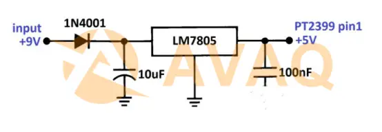
The circuit above shows an effective solution for the PT2399 power supply. Using a 1N4001 diode for protection against accidental polarity connections and 2 capacitors to filter the input/output, the LM7805/LM2940 can accept a wide range of input voltages (+9V to +15V).
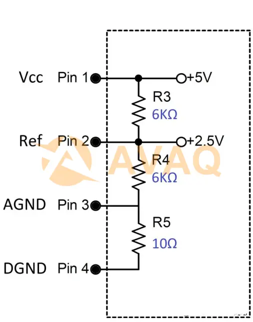
2. Pin 2
Marked REF, is a 2.5 V analog reference voltage (Vcc/2). This voltage is set using an internal resistor divider, with a measured pin resistance of approximately 6 KΩ. This voltage is used as a virtual ground within the PT2399 and as a reference voltage for the VCO circuit.
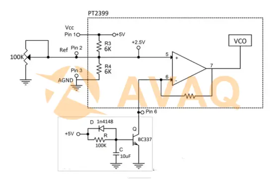
Pin 2 Modulation Modification:
For choir use, the PT2399 internal circuit looks like this:
The VCO (Voltage Controlled Oscillator) voltage will control the delay time of the PT2399: VCO frequency versus delay time, with the delay time being the smallest (31.3ms) when the frequency of this oscillator is at its maximum (22MHz) and vice versa.
If we want to modify the VCO input voltage, the default method is to change the ground resistor on pin 6, which will change the op-amp gain and then the output voltage.
"Pin 2" basically changes the voltage on op-amp pin (+) instead of changing the voltage on pin (-).
In order to do this, the ground resistor on pin 6 needs to be stabilized (usually pin 6 is grounded because it provides the smallest delay time, for this option an "anti-latch circuit" is required) To do this, we can access the internal resistor divider (pin 2) and modulate it.
The bad thing is that the entire virtual ground (2.5V) of the circuit will change with time modulation. The good thing is that we don't need a large span of modulation to create the chorus effect, so changing the voltage on pin 2 from 2.5V to 2V will be enough to create the time modulation and keep the virtual ground good.
3. Pin 3 and Pin 4
are analog and digital ground, respectively, and need to be connected externally with short, thick traces. Measured with a multimeter, an external resistance of 10Ω is shown between the pins.
4. Pin 5
Pin 5 is the system clock output pin (the clock frequency is generated by the VCO in the Pin 2 section).
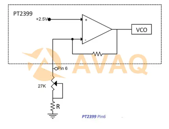
5. Pin 6
VCO (Voltage Controlled Oscillator) frequency adjustment pin. The voltage on this pin is always 2.5V, and the current changes when grounded with an external resistor, resulting in a change in VCO and a change in delay time.
There are several ways to set the delay time using pin 6:
1) Using a potentiometer
This is the simplest method and it is recommended to use an external potentiometer of 10K ~ 50K (depending on the maximum delay time required). A minimum resistor (R) of 2K is always required (it will limit the minimum delay time), otherwise the PT2399 will latch during the power-up sequence and the internal oscillator will not start.

Once the oscillator is started, a minimum resistance (R) of 2K is not required, which is why many designs include anti-latch circuitry, so the system is started with a high impedance on pin 6 and then powered up so that the PT2399 can achieve a shorter delay time. There is no substantial benefit to grounding pin 6, and using a resistor of less than 100 ohms will only result in an increased current demand, not a shorter delay time.
2) Using a Transistor to Limit the Amount of Current Out of Pin 6
PNP or NPN transistors can be used to limit pin current. This method can be used in conjunction with an anti-latch module to ensure that the system will operate under all conditions.
The basic circuit (a) will limit the current out of pin 6: Resistor R1 is needed so that the potentiometer range can be limited to supply 0 to 0.65V to the base of the transistor (otherwise the potentiometer will not work). will only apply to a small part of its entire span).R2 can be any small resistor from 100 to 200Ω.
The second (b) circuit uses a resistor in parallel so that the maximum resistance of pin6 can be controlled and thus the maximum delay time to be used can be better controlled. I.e. using a 20K R3 will give us a maximum of 270ms (follow the datasheet).
Finally (c) Schematic The anti-latch circuit is added so we make sure that the circuit is always activated under any conditions (in case the potentiometer is at its maximum position during the pedal energization period (the first 400ms), setting Q1 to ON and showing a low impedance to pin6.
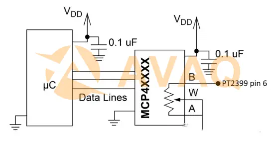
3) Digital Resistors
If you want to include a microcontroller, there are many digital resistors that can be used as variable resistors: microchips MCP41XXX series (256 taps), DS1804 series (100 taps). The downside of this solution is that digital resistors have a large tolerance (±20%) and may not be the most accurate device if you want to set a specific delay time.
PT2399 Block Diagram

PT2399 IC Datasheet PDF
Free download PT2399 IC Datasheet PDF here>>
PT2399 IC Alternative
Coolaudio V3205: This is often considered a direct replacement for the PT2399 and provides similar functionalities for creating delay effects.
MN3005 and MN3205: These are older BBD (Bucket Brigade Device) chips that were used in classic analog delay pedals.
PT2395: It's a variation of the PT2399 with extended delay time and a few other modifications.
BELTON BTDR-2H: While not an IC, the BTDR-2H is a digital reverb module that can be used similarly for creating reverberation and delay effects.
PT2399 IC Manufacturer
The PT2399 is manufactured by Princeton Technology Corporation, a semiconductor company based in Taiwan. They specialize in producing various integrated circuits for audio-related applications which is commonly used in audio effects pedals and other audio processing devices to create delay effects.
Next Industry Focus
CA3080 vs LM13700: Exploring the Differences and How to Choose
 Update Time: Nov 29, 2023 Consumer Electronics
 FAQ
FAQ
- Does the PT2399 offer additional features besides echo effects?
- While the PT2399 is primarily designed for echo effects, it also allows adjustment of the dry/wet mix, making it versatile for audio processing applications.
- Can the PT2399 generate different types of echo effects?
- It allows control over parameters such as delay time, feedback, and mix level, enabling users to create various echo effects, from short slap-back echoes to longer delays.
- What voltage levels does the PT2399 operate with?
- It typically operates with a supply voltage ranging from 5V to 12V.
- How does the PT2399 generate echo or delay effects?
- It uses digital signal processing techniques to sample and delay an input audio signal, creating an echo or delayed output.
Related Industry Focus
-
JRC4558 vs TL072: What are Differences and How to Choose
In this article, we will compare and contrast the JRC4558 and TL072 op-amps, exploring their features, specifications, and applications to guide your selection process for various audio-related projects.
Published: 2023-11-24 18:12:00 -
VIPER12A IC Pinout, Circuit, Datasheet and Equivalent (Pin Video Attached)
The VIPER12A stands as a comprehensive SMPS controller IC featuring an integrated PWM controller paired with a potent power MOSFET on a single silicon chip. This integration enables efficient conversion of a wide AC input voltage range spanning from 85V to 265V into low...
Published: 2023-11-22 16:29:02 -
![KSC1845 Transistor: Equivalent, Datasheet and Pinout [FAQs]](/files/uploads/technology/b/20231120174333ksc1845 transistor-pinout.webp)
KSC1845 Transistor: Equivalent, Datasheet and Pinout [FAQs]
The KSC1845 belongs to the NPN transistor family, a type of bipolar junction transistor commonly packaged in TO-92 format and crafted from silicon semiconductor material.
Published: 2023-11-20 17:45:55 -
Monolithic IC: Overview, Features and Application 2023
A monolithic integrated circuit (IC) is a complete electronic circuit or a group of circuits manufactured on a single piece of silicon, typically around 1.25 mm square (or approximately fifty thousandths of an inch square).
Published: 2023-11-15 18:27:47
PT2399 In Stock: 4734 $0.386
 Popular Industry Focus
Related Parts
-
JL82599EB SR1W7
Intel Corp
Ethernet CTLR Single Chip 1000Mbps/10000Mbps 1.2V/3.3V 576-Pin FCBGA
-
CXD9450-13
Synaptics Incorporated
Single-Chip Fax Engine Product Family
-
KSZ8841-16MBL
Microchip Technology, Inc
Ethernet MAC Controller 10/100 Base-T/TX PHY PCI Interface
-
SARA-G300-00S
U-BLOX AG
GSM/GPRS Cellular Module 900MHz/1800MHz M2M
-
DS3884AVF
Rochester Electronics Incorporated
BTL HANDSHAKE TRANSCEIVER
-
ST20196
STMicroelectronics, Inc
Modem Chip Chipset 24Mbps 208-Pin LBGA
-
LAN91C93I-MC
Microchip Technology, Inc
Ethernet CTLR Single Chip 10Mbps 3.3V/5V 100-Pin QFP
-
UCC3750DWTRG4
Texas Instruments, Inc
Telecom Ringers Source Ringer Controller
-
XLR73234XLPD1000
Broadcom Corporation
Network Controller & Processor ICs XLR732 C4 1.0GHz LP Ind Processor LF
-
LAN91C113-NC
Microchip Technology, Inc
Ethernet CTLR Single Chip 10Mbps/100Mbps 3.3V 128-Pin QFP
-
KSZ8842-PMBL-TR
Microchip Technology, Inc
Ethernet Switch 10/100 Base-T/TX PHY PCI Interface 100-LFBGA (9x9)
-
ST7580TR
STMicroelectronics, Inc
FSK, PSK multi-mode power line networking system-on-chip
-
GX3290-CBE3
Semtech Corporation
Video Switch IC Logic 2377-FCBGA (50x50) Package
-
NH82580DB SLH5U
Intel Corp
Ethernet CTLR Single Chip 10Mbps/100Mbps/1000Mbps 3.3V 256-Pin PBGA
-
TLK1501IRCP
Texas Instruments, Inc
0.6 to 1.5-Gbps transceiver
Featured Manufacturers