Payment Method


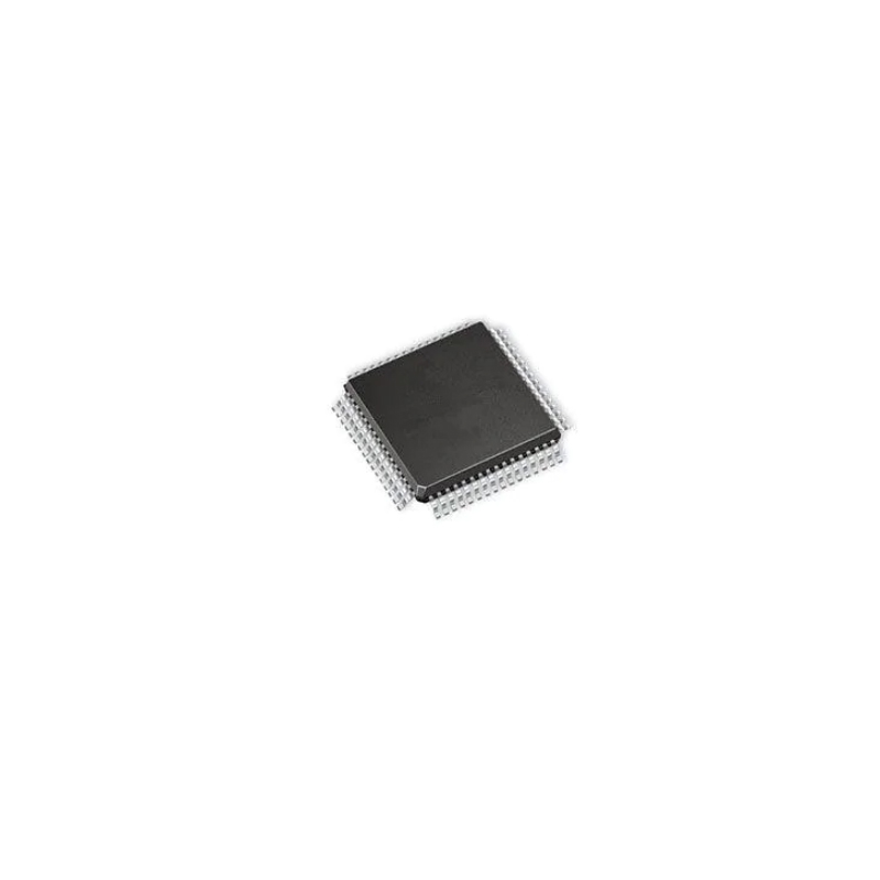
DSP Floating-Point 32bit 140MHz 1120MIPS 429-Pin CFCBGA Tray
429-BCBGA,FCBGAManufacturer:
Texas Instruments
Mfr.Part #:
SM320C6701GLPW14
Datasheet:
Type:
Floating Point
Interface:
DMA, EMIF, HPI, McBSP, SPI
Clock Rate:
140MHz
Non-Volatile Memory:
128kB
EDA/CAD Models:
Please fill in the short form below and we will provide you the quotation immediately.
The SMJ320C67x DSPs are the floating-point DSP family in the SMJ320C6000 platform. The SMJ320C6701 (C6701) device is based on the high-performance, advanced VelociTI very-long-instruction-word (VLIW) architecture developed by Texas Instruments (TI), making this DSP an excellent choice for multichannel and multifunction applications. With performance of up to 1 giga floating-point operations per second (GFLOPS) at a clock rate of 167 MHz, the C6701 offers cost-effective solutions to high-performance DSP programming challenges. The C6701 DSP possesses the operational flexibility of high-speed controllers and the numerical capability of array processors. This processor has 32 general-purpose registers of 32-bit word length and eight highly independent functional units. The eight functional units provide four floating-/fixed-point ALUs, two fixed-point ALUs, and two floating-/fixed-point multipliers. The C6701 can produce two multiply-accumulates (MACs) per cycle for a total of 334 million MACs per second (MMACS). The C6701 DSP also has application-specific hardware logic, on-chip memory, and additional on-chip peripherals.
The C6701 includes a large bank of on-chip memory and has a powerful and diverse set of peripherals. Program memory consists of a 64K-byte block that is user-configurable as cache or memory-mapped program space. Data memory consists of two 32K-byte blocks of RAM. The peripheral set includes two multichannel buffered serial ports (McBSPs), two general-purpose timers, a host-port interface (HPI), and a glueless external memory interface (EMIF) capable of interfacing to SDRAM or SBSRAM and asynchronous peripherals.
The C6701 has a complete set of development tools which includes: a new C compiler, an assembly optimizer to simplify programming and scheduling, and a Windows. debugger interface for visibility into source code execution.
IEEE Standard 1149.1-1990 Standard-Test-Access Port and Boundary Scan Architecture.
VelociTI is a trademark of Texas Instruments Incorporated.
Motorola is a trademark of Motorola, Inc.
TI is a trademark of Texas Instruments Incorporated.
Windows is a registered trademark of the Microsoft Corporation.
| Series | - | Type | Floating Point |
| Interface | DMA, EMIF, HPI, McBSP, SPI | Clock Rate | 140MHz |
| Non-Volatile Memory | 128kB | On-Chip RAM | 128kB |
| Voltage - I/O | 3.30V | Voltage - Core | 1.9V |
| Operating Temperature | -55°C ~ 115°C (TC) | Mounting Type | Surface Mount |
After-Sales & Settlement Related
 Payment
Payment Method


For alternative payment channels, please reach out to us at:
[email protected] Shipping & Packing
Shipping Method


AVAQ determines and packages all devices based on electrostatic discharge (ESD) and moisture sensitivity level (MSL) protection requirements.
 Warranty

365-Day Product
Quality Guarantee
We promise to provide 365 days quality assurance service for all our products.
| Qty. | Unit Price | Ext. Price |
|---|---|---|
| 1+ | - | - |
The prices below are for reference only.
All bill of materials (BOM) can be sent via email to ![]() [email protected],
or fill below form to Quote for SM320C6701GLPW14, guaranteed quotes back within
[email protected],
or fill below form to Quote for SM320C6701GLPW14, guaranteed quotes back within
![]() 12hr.
12hr.

PICASO
4D Systems
Processors - Application Specialized Embedded Serial Graphics Controller

NE555
Texas Instruments
100kHz SOP-8 Timers / Clock Oscillators ROHS

0123456789
HARRIS

74LS04
Onsemi
Inverter IC 6 Channel 14-MDIP

CD21
Cirrus Logic
CD21 deficiency linked to hypogammaglobulinemia and reduced memory B cells