Payment Method


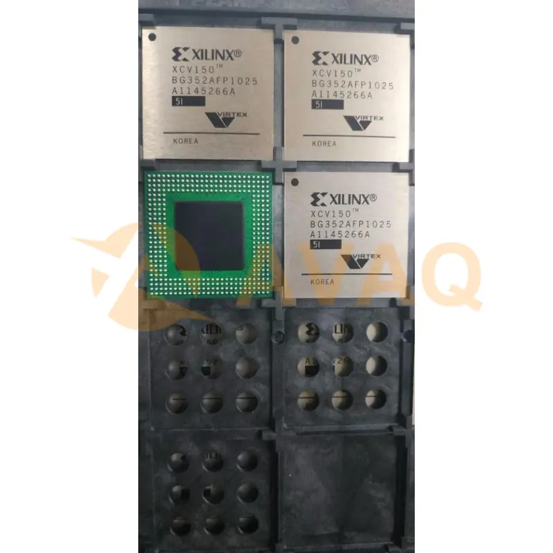
FPGA - Field Programmable Gate Array
Manufacturer:
Mfr.Part #:
XCV150-5BG352I
Datasheet:
Pbfree Code:
No
Part Life Cycle Code:
Obsolete
Pin Count:
352
Reach Compliance Code:
not_compliant
EDA/CAD Models:
Please fill in the short form below and we will provide you the quotation immediately.
Virtex® Field Programmable Gate Array (FPGA) IC 260 49152 3888 352-LBGA Exposed Pad, Metal
| Pbfree Code | No | Part Life Cycle Code | Obsolete |
| Pin Count | 352 | Reach Compliance Code | not_compliant |
| HTS Code | 8542.39.00.01 | Clock Frequency-Max | 294 MHz |
| Combinatorial Delay of a CLB-Max | 0.7 ns | JESD-30 Code | S-PBGA-B352 |
| JESD-609 Code | e0 | Length | 35 mm |
| Moisture Sensitivity Level | 3 | Number of CLBs | 864 |
| Number of Equivalent Gates | 164674 | Number of Inputs | 260 |
| Number of Logic Cells | 3888 | Number of Outputs | 260 |
| Number of Terminals | 352 | Organization | 864 CLBS, 164674 GATES |
| Peak Reflow Temperature (Cel) | 225 | Programmable Logic Type | FIELD PROGRAMMABLE GATE ARRAY |
| Qualification Status | Not Qualified | Seated Height-Max | 1.7 mm |
| Supply Voltage-Max | 2.625 V | Supply Voltage-Min | 2.375 V |
| Supply Voltage-Nom | 2.5 V | Surface Mount | YES |
| Technology | CMOS | Terminal Finish | Tin/Lead (Sn63Pb37) |
| Terminal Form | BALL | Terminal Pitch | 1.27 mm |
| Terminal Position | BOTTOM | Time@Peak Reflow Temperature-Max (s) | 30 |
| Width | 35 mm |
After-Sales & Settlement Related
 Payment
Payment Method


For alternative payment channels, please reach out to us at:
[email protected] Shipping & Packing
Shipping Method


AVAQ determines and packages all devices based on electrostatic discharge (ESD) and moisture sensitivity level (MSL) protection requirements.
 Warranty

365-Day Product
Quality Guarantee
We promise to provide 365 days quality assurance service for all our products.
| Qty. | Unit Price | Ext. Price |
|---|---|---|
| 1+ | - | - |
The prices below are for reference only.
All bill of materials (BOM) can be sent via email to ![]() [email protected],
or fill below form to Quote for XCV150-5BG352I, guaranteed quotes back within
[email protected],
or fill below form to Quote for XCV150-5BG352I, guaranteed quotes back within
![]() 12hr.
12hr.
