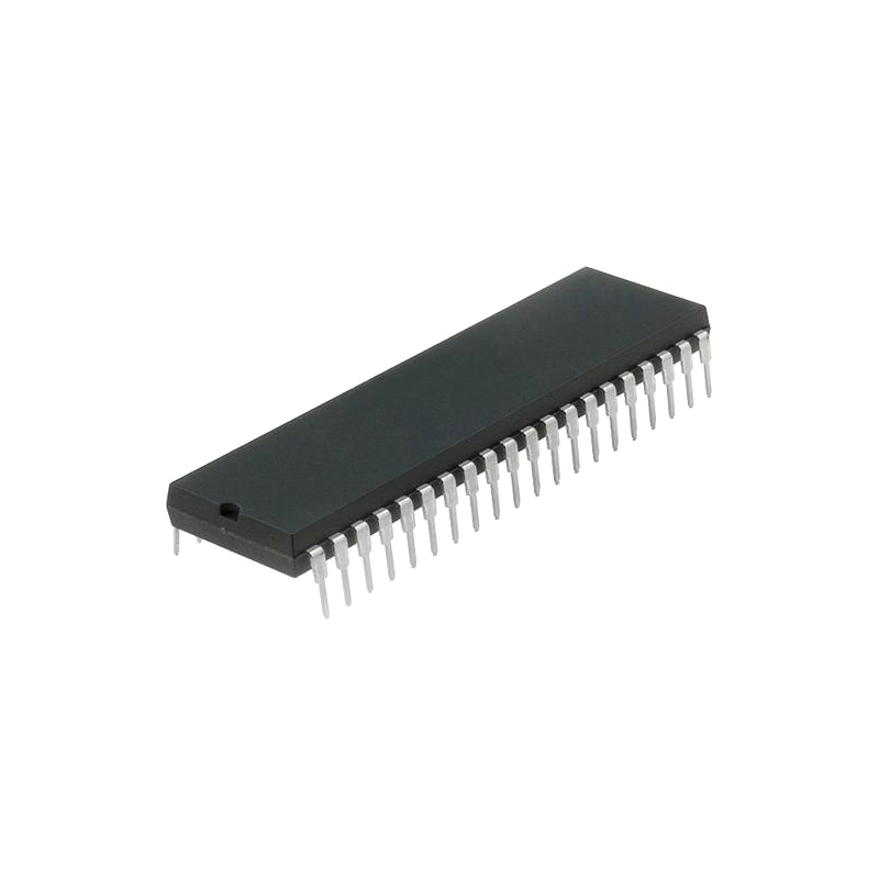
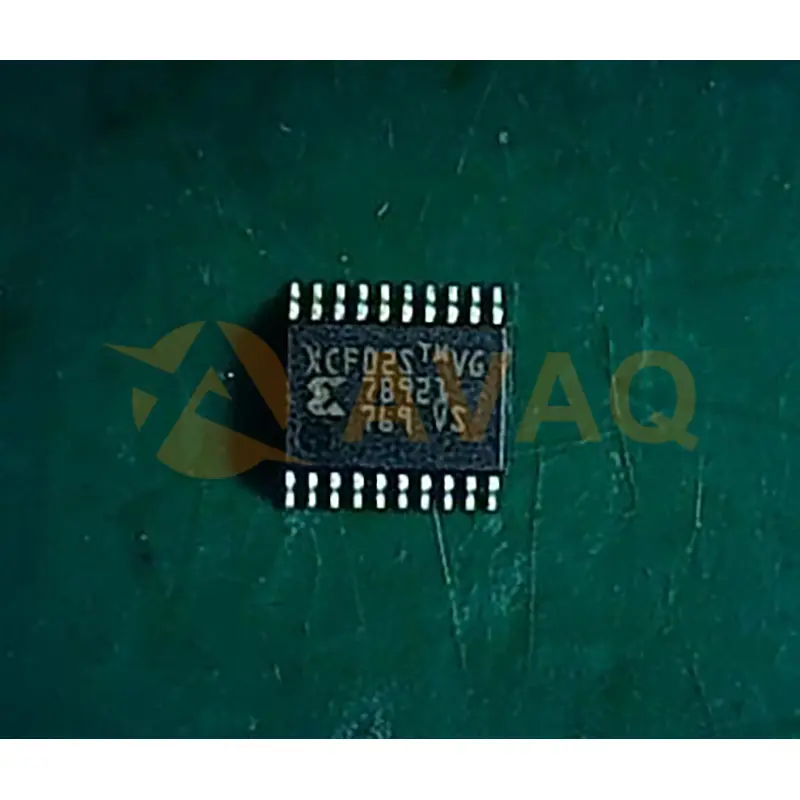
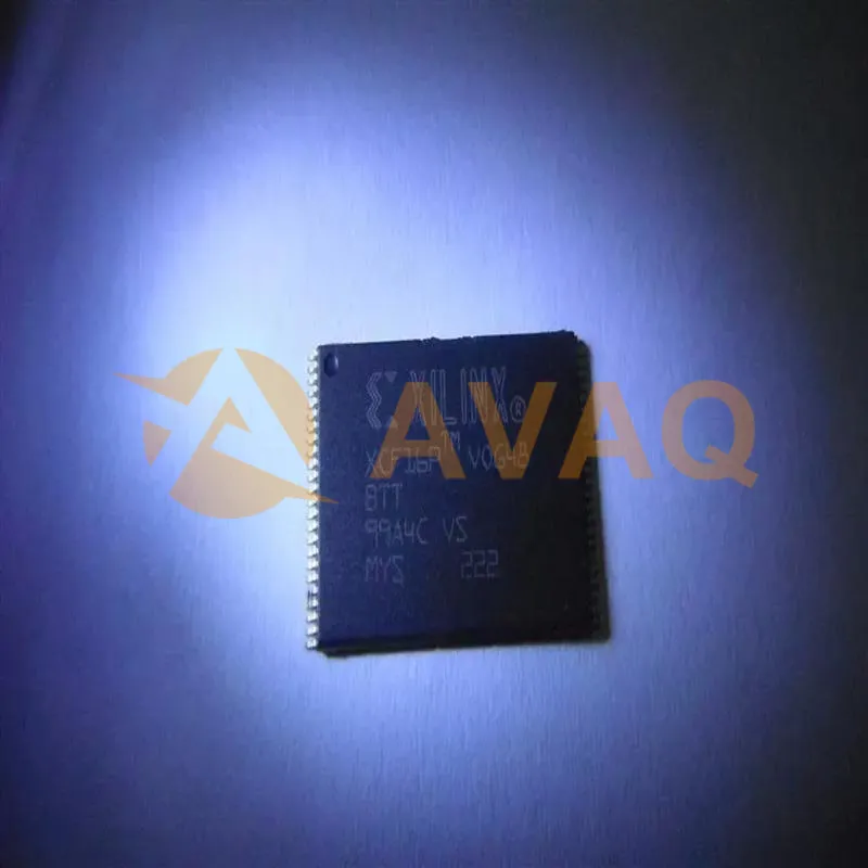
XC17V08PC44C General Description
Xilinx introduces the high-density XC17V00 family of configuration PROMs which provide an easy-to-use, costeffective method for storing large Xilinx FPGA configuration bitstreams. Initial devices in the 3.3V family are available in 16 Mb, 8 Mb, 4 Mb, 2 Mb, and 1 Mb densities. See Figure 1 and Figure 2 for simplified block diagrams of the XC17V00 family.
The XC17V00 PROM can configure a Xilinx FPGA using the FPGA serial configuration mode interface. When the FPGA is in Master Serial mode, it generates a configuration clock that drives the PROM. A short access time after the rising clock edge, data appears on the PROM DATA output pin that is connected to the FPGA DIN pin. The FPGA generates the appropriate number of clock pulses to complete the configuration. Once configured, it disables the PROM. When the FPGA is in Slave Serial mode, the PROM and the FPGA must both be clocked by an incoming signal.
The XC17V08(1) and XC17V16 PROM can optionally configure a Xilinx FPGA using the FPGA Parallel (SelectMAP) configuration mode interface. When the FPGA is in Master SelectMAP mode, the FPGA generates the configuration clock that drives the PROM.
When the FPGA is in Slave SelectMAP mode, an external, free-running oscillator generates the configuration clock that drives the PROM and the FPGA. After the rising configuration clock (CCLK) edge, data is available on the PROMs DATA (D0-D7) pins. The data is clocked into the FPGA on the following rising edge of the CCLK (Figure 3).
Multiple PROMs can be concatenated by using the CEO output to drive the CE input of the following device. The clock inputs and the DATA outputs of all PROMs in this chain are interconnected. All devices are compatible and can be cascaded with other members of the family.
For device programming, either the Xilinx ISE Foundation or ISE WebPACK software compiles the FPGA design file into a standard Hex format, which is then transferred to most commercial PROM programmers.

 Payment


 Shipping & Packing


 Warranty