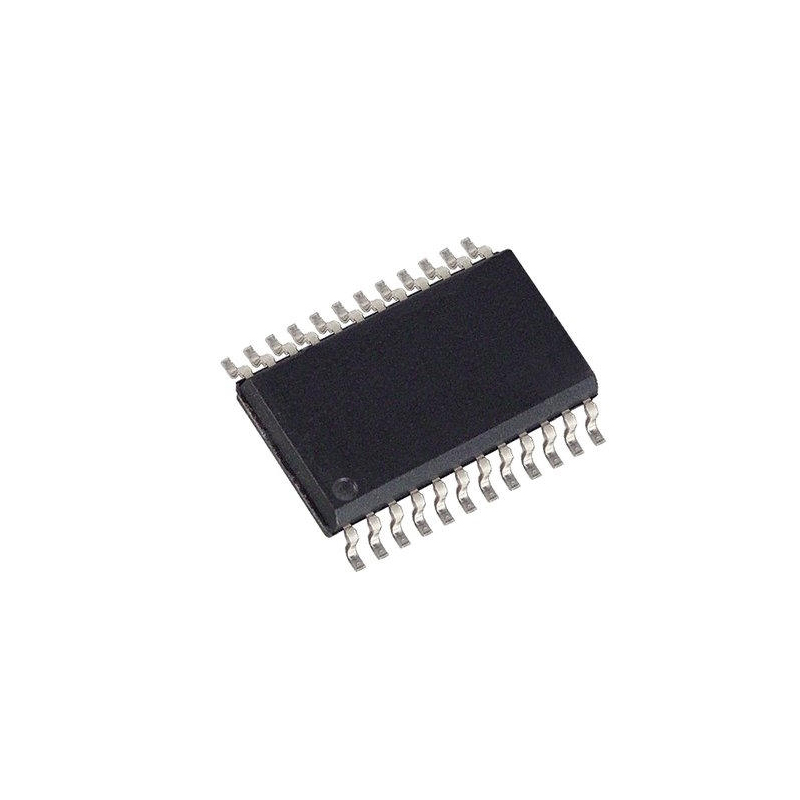
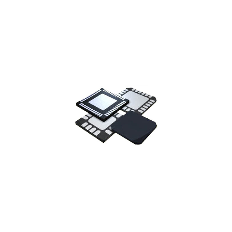
SN65LVDS822RGZR General Description
The SN65LVDS822 is an advanced FlatLink™ low-voltage differential signal (LVDS) receiver designed on a modern CMOS process. The device has several unique features, including three selectable CMOS output slew rates, CMOS output voltage support of 1.8 V to 3.3 V, a pinout swap option, integrated differential termination (configurable), an automatic low-power mode, and deserialization modes of 4:27 and 2:27. The device is compatible with TI FlatLink™ transmitters such as the SN75LVDS83B, SN65LVDS93A, and standard industry LVDS transmitters that comply with TIA/EIA 644-A.
The SN65LVDS822 features an automatic low-power Standby Mode, activated when the LVDS clock is disabled. The device enters an even lower-power Shutdown Mode with a low voltage applied to pin SHTDN#.
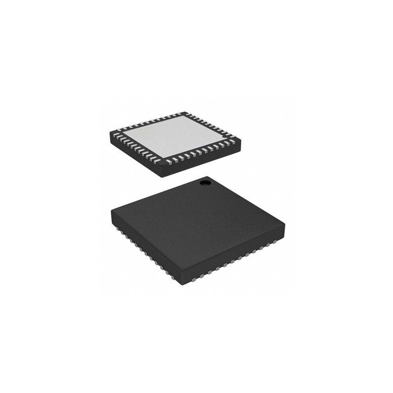
The SN65LVDS822 is packaged in a 48-pin 7-mm × 7-mm Plastic Quad Flatpack No-Lead (QFN) with a 0.5-mm pin pitch, and operates through an industrial ambient temperature range of 40°C to 85°C.
A clock frequency range of 4 MHz to 54 MHz is supported in the standard 7× mode, which is to be used with LVDS data rates of 28 Mbps to 378 Mbps. The 14x mode supports 4 MHz to 27 MHz, for LVDS data rates of 56Mbps to 378 Mbps. The LVDS clock frequency always matches the CMOS output clock frequency. DC common mode voltage is monitored on clock line for normal operation. The device is designed to support resolutions as low as 1/16th VGA (160 × 120), and as high as 1024 × 600, with 60 frames per second and 24-bit color.
The SN65LVDS822 features an automatic low-power standby mode, activated when the LVDS clock is disabled. The device enters an even lower-power shutdown mode with a low voltage applied to pin SHTDN#. In both low-power modes, all CMOS outputs drive low. All input pins have fail-safe protection that prevents damage from occurring before power supply voltages are high and stable.
The SN65LVDS822 is packaged in a 48-pin 7-mm x 7-mm Plastic Quad Flatpack No-Lead (QFN) with a 0.5-mm pin pitch, and operates through an industrial ambient temperature range of 40°C to 85°C.


 Payment


 Shipping & Packing


 Warranty