Payment Method


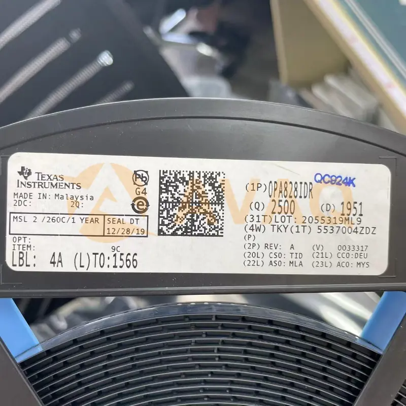
J-FET Amplifier 1 Circuit 8-SOIC
Manufacturer:
Mfr.Part #:
OPA828IDR
Datasheet:
Number of channels:
1
Total supply voltage (+5 V = 5, ±5 V = 10) (max) (V):
36
Total supply voltage (+5 V = 5, ±5 V = 10) (min) (V):
8
Vos (offset voltage at 25°C) (max) (mV):
0.3
EDA/CAD Models:
Please fill in the short form below and we will provide you the quotation immediately.
The OPA828 and OPA2828 ( OPAx828) JFET input operational amplifiers are the next generation OPA627 and OPA827, combining high speed with high dc precision and ac performance. These op amps supply low offset voltage, low drift over temperature, low bias current, and low noise with only 60-nVRMS 0.1-Hz to 10-Hz noise. The OPAx828 operate over a wide supply-voltage range of ±4 V to ±18 V and a supply current of 5.5 mA/channel, typical.
AC characteristics, including a 45-MHz gain bandwidth product (GBW), a slew rate of 150 V/µs, and precision dc characteristics, make the OPAx828 family an excellent choice for a variety of systems. These include high-speed and high-resolution data-acquisition systems, such as 16-bit to 18-bit mixed signal systems, transimpedance (I/V-conversion) amplifiers, filters, precision ±10-V front ends, and high-impedance sensor-interface applications.
The OPAx828 are available in an 8-pin SOIC package and a thermally enhanced, 8-pin HVSSOP PowerPAD™ integrated circuit package.
| Number of channels | 1 | Total supply voltage (+5 V = 5, ±5 V = 10) (max) (V) | 36 |
| Total supply voltage (+5 V = 5, ±5 V = 10) (min) (V) | 8 | Vos (offset voltage at 25°C) (max) (mV) | 0.3 |
| GBW (typ) (MHz) | 45 | Features | MUX Friendly |
| Slew rate (typ) (V/µs) | 150 | Rail-to-rail | Out |
| Offset drift (typ) (µV/°C) | 0.3 | Iq per channel (typ) (mA) | 5.5 |
| Vn at 1 kHz (typ) (nV√Hz) | 4 | CMRR (typ) (dB) | 115 |
| Rating | Catalog | Operating temperature range (°C) | -40 to 125 |
| Input bias current (max) (pA) | 8 | Iout (typ) (A) | 0.03 |
| Architecture | FET | Input common mode headroom (to negative supply) (typ) (V) | 2.5 |
| Input common mode headroom (to positive supply) (typ) (V) | -3.5 | Output swing headroom (to negative supply) (typ) (V) | 0.9 |
| Output swing headroom (to positive supply) (typ) (V) | -0.9 | THD + N at 1 kHz (typ) (%) | 0.000028 |
After-Sales & Settlement Related
 Payment
Payment Method


For alternative payment channels, please reach out to us at:
[email protected] Shipping & Packing
Shipping Method


AVAQ determines and packages all devices based on electrostatic discharge (ESD) and moisture sensitivity level (MSL) protection requirements.
 Warranty

365-Day Product
Quality Guarantee
We promise to provide 365 days quality assurance service for all our products.
| Qty. | Unit Price | Ext. Price |
|---|---|---|
| 1+ | $5.347 | $5.35 |
| 10+ | $4.670 | $46.70 |
| 30+ | $4.257 | $127.71 |
| 100+ | $3.911 | $391.10 |
The prices below are for reference only.
All bill of materials (BOM) can be sent via email to ![]() [email protected],
or fill below form to Quote for OPA828IDR, guaranteed quotes back within
[email protected],
or fill below form to Quote for OPA828IDR, guaranteed quotes back within
![]() 12hr.
12hr.
