Payment Method


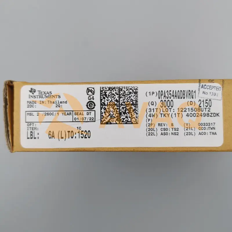
Automotive 250MHz, Rail-to-Rail I/O, CMOS Single Operational Amplifier
Manufacturer:
Mfr.Part #:
OPA354AQDBVRQ1
Datasheet:
Architecture:
FET / CMOS Input, Voltage FB
Number of channels:
1
Total supply voltage (+5 V = 5, ±5 V = 10) (min) (V):
2.5
Total supply voltage (+5 V = 5, ±5 V = 10) (max) (V):
5.5
EDA/CAD Models:
Please fill in the short form below and we will provide you the quotation immediately.
The design of the OPAx354-Q1 family of high-speed, voltage-feedback CMOS operational amplifiers is for video and other applications requiring wide bandwidth. These devices are unity-gain stable and can drive large output currents. Differential gain is 0.02% and differential phase is 0.09°. Quiescent current is only 4.9 mA per channel.
The OPAx354-Q1 family of operational amplifiers (op-amps) are optimized for operation on single or dual supplies as low as 2.5 V (±1.25 V) and up to 5.5 V (±2.75 V). Common-mode input range extends beyond the supplies. The output swing is within 100 mV of the rails, supporting wide dynamic range.
The single-supply version (OPA354A-Q1) is available in the tiny SOT–23-5 (DBV) package. The dual-supply version (OPA2354A-Q1) is available in the miniature VSSOP-8 (DGK) package and features completely independent circuitry for lowest crosstalk and freedom from interaction. The quad-supply version (OPA4354-Q1) is available in the TSSOP-14 (PW) package. The device specifications are for operation over the automotive temperature range of –40°C to +125°C.
| Architecture | FET / CMOS Input, Voltage FB | Number of channels | 1 |
| Total supply voltage (+5 V = 5, ±5 V = 10) (min) (V) | 2.5 | Total supply voltage (+5 V = 5, ±5 V = 10) (max) (V) | 5.5 |
| GBW (typ) (MHz) | 100 | BW at Acl (MHz) | 250 |
| Acl, min spec gain (V/V) | 1 | Slew rate (typ) (V/µs) | 150 |
| Vn at flatband (typ) (nV√Hz) | 6.5 | Vn at 1 kHz (typ) (nV√Hz) | 6.5 |
| Iq per channel (typ) (mA) | 4.9 | Vos (offset voltage at 25°C) (max) (mV) | 8 |
| Rail-to-rail | In, Out | Rating | Automotive |
| Operating temperature range (°C) | -40 to 125 | CMRR (typ) (dB) | 80 |
| Input bias current (max) (pA) | 50 | Offset drift (typ) (µV/°C) | 4 |
| Iout (typ) (mA) | 100 | 2nd harmonic (dBc) | 75 |
| 3rd harmonic (dBc) | 83 | Frequency of harmonic distortion measurement (MHz) | 1 |
After-Sales & Settlement Related
 Payment
Payment Method


For alternative payment channels, please reach out to us at:
[email protected] Shipping & Packing
Shipping Method


AVAQ determines and packages all devices based on electrostatic discharge (ESD) and moisture sensitivity level (MSL) protection requirements.
 Warranty

365-Day Product
Quality Guarantee
We promise to provide 365 days quality assurance service for all our products.
| Qty. | Unit Price | Ext. Price |
|---|---|---|
| 1+ | $1.548 | $1.55 |
| 10+ | $1.344 | $13.44 |
| 30+ | $1.217 | $36.51 |
| 100+ | $1.042 | $104.20 |
| 500+ | $0.983 | $491.50 |
| 1000+ | $0.956 | $956.00 |
The prices below are for reference only.
All bill of materials (BOM) can be sent via email to ![]() [email protected],
or fill below form to Quote for OPA354AQDBVRQ1, guaranteed quotes back within
[email protected],
or fill below form to Quote for OPA354AQDBVRQ1, guaranteed quotes back within
![]() 12hr.
12hr.

Received quickly. the number did not count.