Payment Method


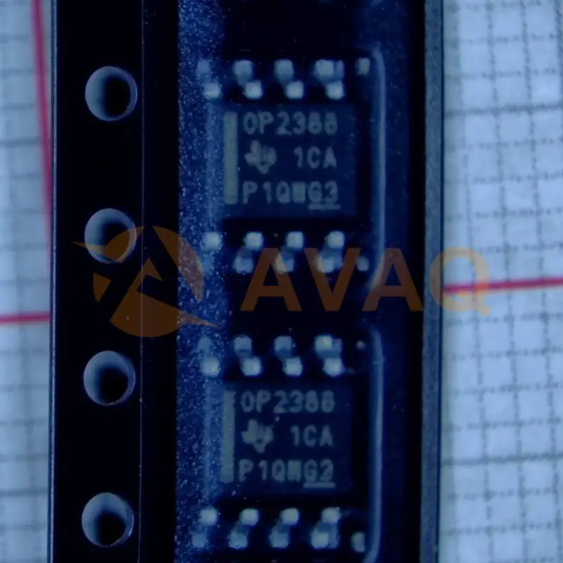
Op Amp Dual Zero Drift Amplifier R-R I/O ±2.75V/5.5V 8-Pin SOIC T/R
Manufacturer:
Mfr.Part #:
OPA2388IDR
Datasheet:
Pbfree Code:
Yes
Part Life Cycle Code:
Active
Reach Compliance Code:
compliant
Date Of Intro:
2017-06-22
EDA/CAD Models:
Please fill in the short form below and we will provide you the quotation immediately.
The OPAx388 (OPA388, OPA2388, and OPA4388) series of precision operational amplifiers are ultra-low noise, fast-settling, zero-drift, zero-crossover devices that provide rail-to-rail input and output operation. These features and excellent ac performance, combined with only 0.25 μV of offset and 0.005 μV/°C of drift over temperature, makes the OPAx388 a great choice for driving high-precision, analog-to-digital converters (ADCs) or buffering the output of high-resolution, digital-to-analog converters (DACs). This design results in excellent performance when driving analog-to-digital converters (ADCs) without degradation of linearity. The OPA388 (single version) is available in the VSSOP-8, SOT23-5, and SOIC-8 packages. The OPA2388 (dual version) is offered in the VSSOP-8 and SO-8 packages. The OPA4388 (quad version) is offered in the TSSOP-14 and SO-14 packages. All versions are specified over the industrial temperature range of –40°C to +125°C.
| Source Content uid | OPA2388IDR | Pbfree Code | Yes |
| Part Life Cycle Code | Active | Reach Compliance Code | compliant |
| Date Of Intro | 2017-06-22 | Amplifier Type | OPERATIONAL AMPLIFIER |
| Architecture | VOLTAGE-FEEDBACK | Average Bias Current-Max (IIB) | 0.0007 µA |
| Bias Current-Max (IIB) @25C | 0.00035 µA | Common-mode Reject Ratio-Min | 124 dB |
| Common-mode Reject Ratio-Nom | 140 dB | Frequency Compensation | YES |
| Input Offset Current-Max (IIO) | 0.0008 µA | Input Offset Voltage-Max | 7.5 µV |
| JESD-30 Code | R-PDSO-G8 | JESD-609 Code | e3 |
| Length | 4.9 mm | Low-Bias | YES |
| Low-Offset | YES | Micropower | NO |
| Moisture Sensitivity Level | 2 | Neg Supply Voltage Limit-Max | -3 V |
| Neg Supply Voltage-Nom (Vsup) | -2.5 V | Number of Functions | 2 |
| Number of Terminals | 8 | Operating Temperature-Max | 125 °C |
| Operating Temperature-Min | -40 °C | Peak Reflow Temperature (Cel) | 260 |
| Power | NO | Programmable Power | NO |
| Seated Height-Max | 1.75 mm | Slew Rate-Nom | 5 V/us |
| Supply Current-Max | 4.8 mA | Supply Voltage Limit-Max | 3 V |
| Supply Voltage-Nom (Vsup) | 2.5 V | Surface Mount | YES |
| Temperature Grade | AUTOMOTIVE | Terminal Finish | Matte Tin (Sn) |
| Terminal Form | GULL WING | Terminal Pitch | 1.27 mm |
| Terminal Position | DUAL | Time@Peak Reflow Temperature-Max (s) | NOT SPECIFIED |
| Unity Gain BW-Nom | 10000 | Voltage Gain-Min | 1000000 |
| Wideband | NO | Width | 3.9 mm |
After-Sales & Settlement Related
 Payment
Payment Method


For alternative payment channels, please reach out to us at:
[email protected] Shipping & Packing
Shipping Method


AVAQ determines and packages all devices based on electrostatic discharge (ESD) and moisture sensitivity level (MSL) protection requirements.
 Warranty

365-Day Product
Quality Guarantee
We promise to provide 365 days quality assurance service for all our products.
| Qty. | Unit Price | Ext. Price |
|---|---|---|
| 1+ | - | - |
The prices below are for reference only.
All bill of materials (BOM) can be sent via email to ![]() [email protected],
or fill below form to Quote for OPA2388IDR, guaranteed quotes back within
[email protected],
or fill below form to Quote for OPA2388IDR, guaranteed quotes back within
![]() 12hr.
12hr.
