Payment Method


450 µA, 5 MHz Rail-to-Rail Op Amp.
Manufacturer:
Mfr.Part #:
MCP6281T-E/OT
Datasheet:
Pbfree Code:
Yes
Part Life Cycle Code:
Active
Pin Count:
5
Reach Compliance Code:
compliant
EDA/CAD Models:
Please fill in the short form below and we will provide you the quotation immediately.
The Microchip Technology Inc. MCP6281/1R/2/3/4/5 family of operational amplifiers (op amps) provide wide bandwidth for the current. This family has a 5 MHz Gain Bandwidth Product (GBWP) and a 65° phase margin. This family also operates from a single supply voltage as low as 2.2V, while drawing 450 µA (typical) quiescent current. Additionally, the MCP6281/1R/2/3/4/5 supports rail-to-rail input and output swing, with a common mode input voltage range of VDD + 300mV to VSS – 300 mV. This family of operational amplifiers is designed with Microchip’s advanced CMOS process. The MCP6285 has a Chip Select (CS) input for dual op amps in an 8-pin package. This device is manufactured by cascading the two op amps (the output of op amp A connected to the non-inverting input of op amp B). The CS input puts the device in Low-power mode. The MCP6281/1R/2/3/4/5 family operates over the Extended Temperature Range of -40°C to +125°C. It also has a power supply range of 2.2V to 6.0V.
| Source Content uid | MCP6281T-E/OT | Pbfree Code | Yes |
| Part Life Cycle Code | Active | Pin Count | 5 |
| Reach Compliance Code | compliant | ECCN Code | EAR99 |
| HTS Code | 8542.33.00.01 | Factory Lead Time | 52 Weeks |
| Amplifier Type | OPERATIONAL AMPLIFIER | Architecture | VOLTAGE-FEEDBACK |
| Average Bias Current-Max (IIB) | 0.005 µA | Common-mode Reject Ratio-Min | 65 dB |
| Common-mode Reject Ratio-Nom | 85 dB | Frequency Compensation | YES |
| Input Offset Voltage-Max | 5000 µV | JESD-30 Code | R-PDSO-G5 |
| JESD-609 Code | e3 | Length | 2.9 mm |
| Low-Bias | YES | Low-Offset | NO |
| Micropower | YES | Moisture Sensitivity Level | 1 |
| Number of Functions | 1 | Number of Terminals | 5 |
| Operating Temperature-Max | 125 °C | Operating Temperature-Min | -40 °C |
| Packing Method | TAPE AND REEL | Peak Reflow Temperature (Cel) | 260 |
| Power | NO | Programmable Power | NO |
| Qualification Status | Not Qualified | Seated Height-Max | 1.45 mm |
| Slew Rate-Nom | 2.5 V/us | Supply Current-Max | 0.57 mA |
| Supply Voltage Limit-Max | 7 V | Supply Voltage-Nom (Vsup) | 5 V |
| Surface Mount | YES | Technology | CMOS |
| Temperature Grade | AUTOMOTIVE | Terminal Finish | MATTE TIN |
| Terminal Form | GULL WING | Terminal Pitch | 0.95 mm |
| Terminal Position | DUAL | Unity Gain BW-Nom | 5000 |
| Voltage Gain-Min | 31620 | Wideband | NO |
| Width | 1.6 mm |
After-Sales & Settlement Related
 Payment
Payment Method


For alternative payment channels, please reach out to us at:
[email protected] Shipping & Packing
Shipping Method


AVAQ determines and packages all devices based on electrostatic discharge (ESD) and moisture sensitivity level (MSL) protection requirements.
 Warranty

365-Day Product
Quality Guarantee
We promise to provide 365 days quality assurance service for all our products.
| Qty. | Unit Price | Ext. Price |
|---|---|---|
| 1+ | $0.353 | $0.35 |
| 10+ | $0.287 | $2.87 |
| 30+ | $0.258 | $7.74 |
| 100+ | $0.210 | $21.00 |
| 500+ | $0.195 | $97.50 |
| 1000+ | $0.184 | $184.00 |
The prices below are for reference only.
All bill of materials (BOM) can be sent via email to ![]() [email protected],
or fill below form to Quote for MCP6281T-E/OT, guaranteed quotes back within
[email protected],
or fill below form to Quote for MCP6281T-E/OT, guaranteed quotes back within
![]() 12hr.
12hr.
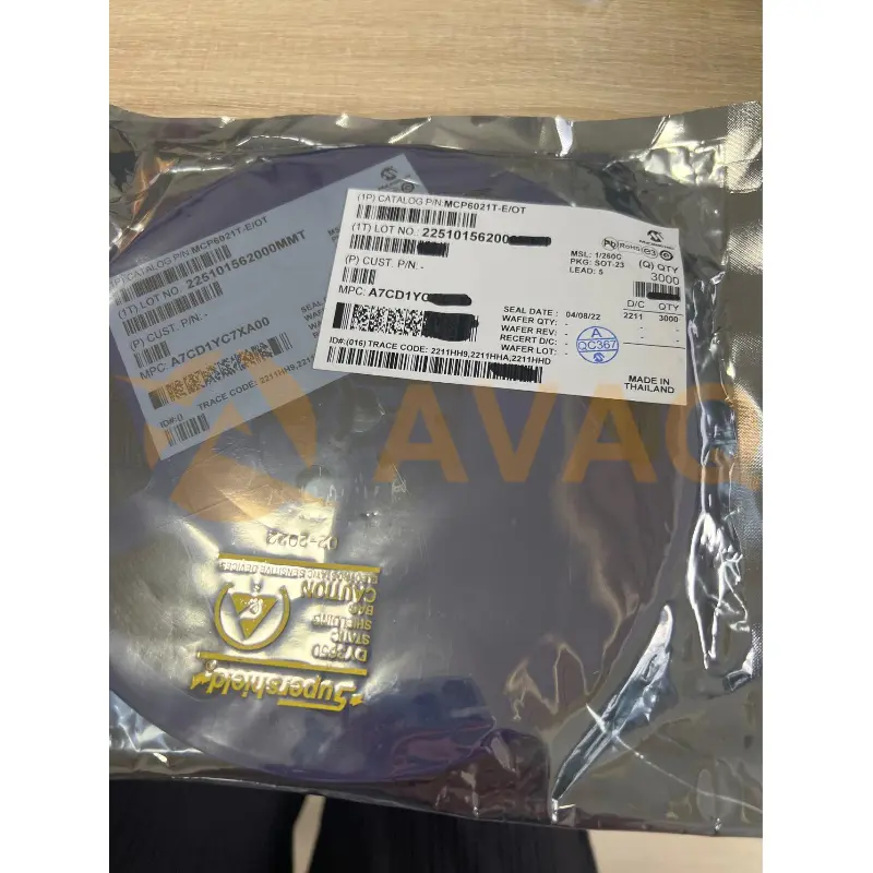
MCP6021T-E/OT
MICROCHIP
1000+ $0.494

MCP602-I/SN
MICROCHIP
1000+ $0.307
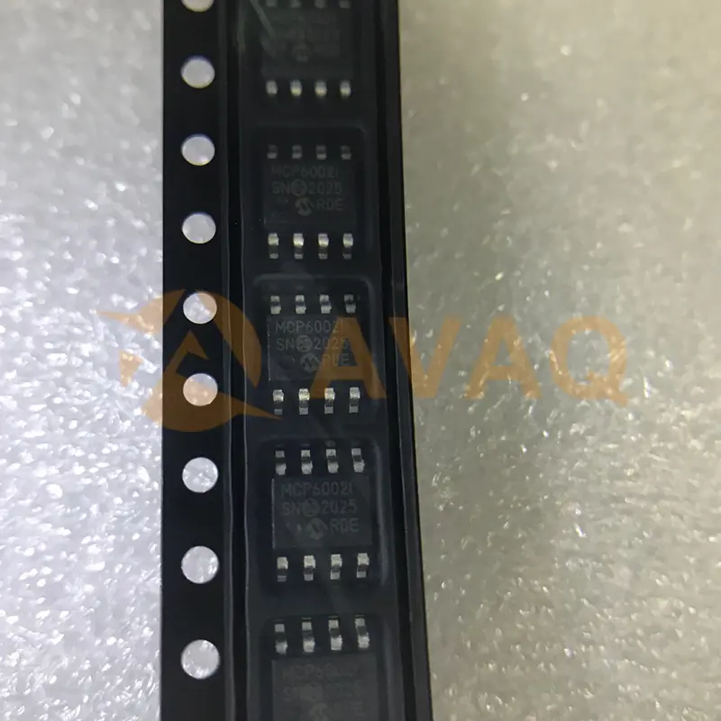
MCP6002T-I/SN
Microchip
6600+ $0.182
MCP6001T-I/OT
Microchip
6000+ $0.142
MCP6002-I/SN
Microchip
With a maximum offset of 4500 uV and a bandwidth of 1 MHz, the MCP6002-I/SN is a dual operational amplifier housed in a PDSO8 package with a 3