Payment Method


Interface - Specialized
Manufacturer:
Mfr.Part #:
HS1-3282-8
Datasheet:
Part Life Cycle Code:
Active
Pin Count:
40
Boundary Scan:
NO
Data Encoding/Decoding Method:
NRZ
Please fill in the short form below and we will provide you the quotation immediately.
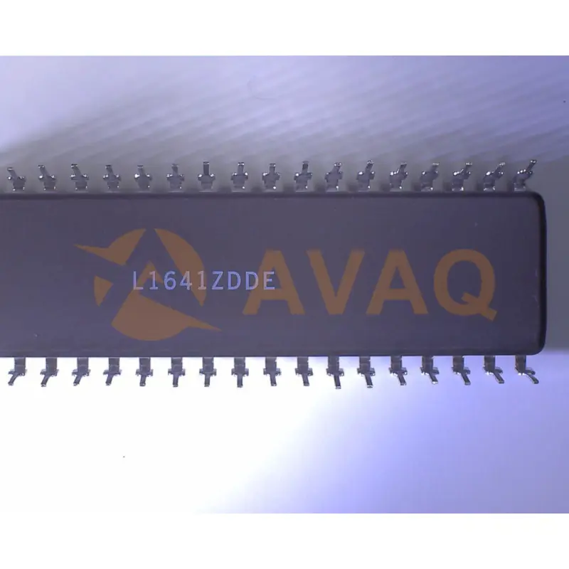
The HS-3282 is a high performance CMOS bus interface circuit that is intended to meet the requirements of ARINC Specification 429, and similar encoded, time multiplexed serial data protocols. This device is intended to be used with the HS-3182, a monolithic Dl bipolar differential line driver designed to meet the specifications of ARINC 429. The ARINC 429 bus interface circuit consists of two (2) receivers and a transmitter operating independently as shown in Figure 1. The two receivers operate at a frequency that is ten (10) times the receiver data rate, which can be the same or different from the transmitter data rate. Although the two receivers operate at the same frequency, they are functionally independent and each receives serial data asynchronously. The transmitter section of the ARINC bus interface circuit consists mainly of a First-In First-Out (FIFO) memory and timing circuit. The FIFO memory is used to hold up to eight (8) ARINC data words for transmission serially. The timing circuit is used to correctly separate each ARINC word as required by ARINC Specification 429. Even though ARINC Specification 429 specifies a 32-bit word, including parity, the HS-3282 can be programmed to also operate with a word length of 25 bits. The incoming receiver data word parity is checked, and a parity status is stored in the receiver latch and output on Pin BD08 during the 1st word. [A logic 0 indicates that an odd number of logic 1 s were received and stored; a logic 1 indicates that an even number of logic 1s were received and stored]. In the transmitter the parity generator will generate either odd or even parity depending upon the status of PARCK control signal. A logic 0 on BD12 will cause odd parity to be used in the output data stream. Versatility is provided in both the transmitter and receiver by the external clock input which allows the bus interface circuit to operate at data rates from 0 to 100 kilobits. The external clock must be ten (10) times the data rate to insure no data ambiguity. The ARINC bus interface circuit is fully guaranteed to support the data rates of ARINC specification 429 over both the voltage (±5%) and full military temperature range. It interfaces with UL, CMOS or NMOS support circuitry, and uses the standard 5-volt VCC supply.
| Part Life Cycle Code | Active | Pin Count | 40 |
| Reach Compliance Code | Address Bus Width | ||
| Boundary Scan | NO | Data Encoding/Decoding Method | NRZ |
| Data Transfer Rate-Max | 0.01220703125 MBps | External Data Bus Width | 16 |
| JESD-30 Code | R-GDIP-T40 | Low Power Mode | YES |
| Number of Serial I/Os | 1 | Number of Terminals | 40 |
| Operating Temperature-Max | 125 °C | Operating Temperature-Min | -55 °C |
| Qualification Status | COMMERCIAL | Supply Voltage-Max | 5.25 V |
| Supply Voltage-Min | 4.75 V | Supply Voltage-Nom | 5 V |
| Surface Mount | NO | Technology | CMOS |
| Temperature Grade | MILITARY | Terminal Form | THROUGH-HOLE |
| Terminal Position | DUAL | uPs/uCs/Peripheral ICs Type | SERIAL IO/COMMUNICATION CONTROLLER, SERIAL |
After-Sales & Settlement Related
 Payment
Payment Method


For alternative payment channels, please reach out to us at:
[email protected] Shipping & Packing
Shipping Method


AVAQ determines and packages all devices based on electrostatic discharge (ESD) and moisture sensitivity level (MSL) protection requirements.
 Warranty

365-Day Product
Quality Guarantee
We promise to provide 365 days quality assurance service for all our products.
| Qty. | Unit Price | Ext. Price |
|---|---|---|
| 1+ | - | - |
The prices below are for reference only.
All bill of materials (BOM) can be sent via email to ![]() [email protected],
or fill below form to Quote for HS1-3282-8, guaranteed quotes back within
[email protected],
or fill below form to Quote for HS1-3282-8, guaranteed quotes back within
![]() 12hr.
12hr.
