Payment Method


Operational Amplifiers - Op Amps
Manufacturer:
INTERSIL/HARRIS
Mfr.Part #:
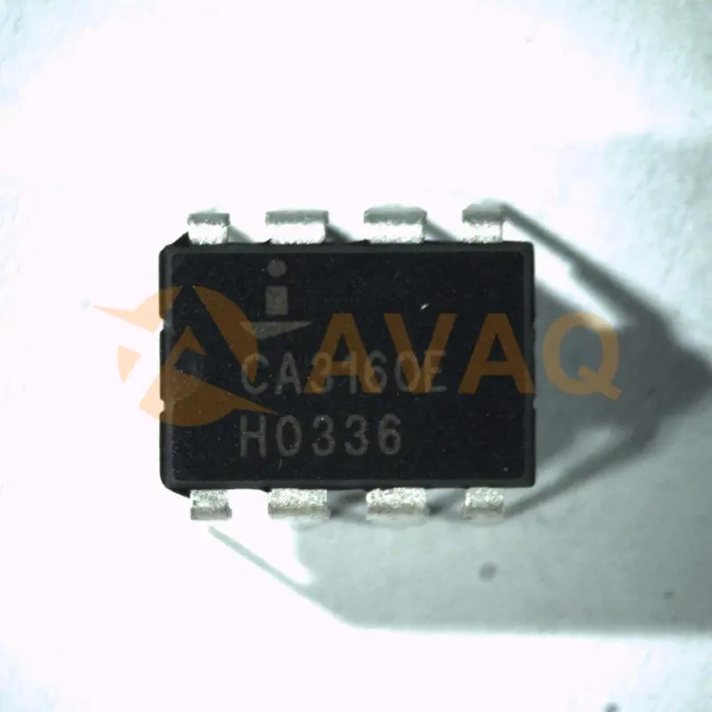
CA3160E
Datasheet:
Part Life Cycle Code:
Transferred
ECCN Code:
EAR99
HTS Code:
8542.33.00.01
Amplifier Type:
OPERATIONAL AMPLIFIER
EDA/CAD Models:
Please fill in the short form below and we will provide you the quotation immediately.
Gate protected P-Channel MOSFET (PMOS) transistors are used in the input circuit to provide very high input impedance, very low input current, and exceptional speed performance. The use of PMOS field effect transistors in the input stage results in common-mode input voltage capability down to 0.5V below the negative supply terminal, an important attribute in single supply applications.
MOSFET Input Stage Provides:
- Very High ZI = 1.5T (1.5 x 10¹²) (Typ)
- Very Low II . . . . . . . . . . . . . 5pA (Typ) at 15V Operation
. . . . . . . . . . . . . . . . . . . . . . . 2pA (Typ) at 5V Operation
Common-Mode Input Voltage Range Includes
Negative Supply Rail; Input Terminals Can Be Swung
0.5V Below Negative Supply Rail
CMOS Output Stage Permits Signal Swing to Either (or Both) Supply Rails
Ground Referenced Single Supply Amplifiers
Fast Sample Hold Amplifiers
Long Duration Timers/Monostables
High Input Impedance Wideband Amplifiers
Voltage Followers (e.g., Follower for Single Supply D/A Converter)
Wien-Bridge Oscillators
Voltage Controlled Oscillators
Photo Diode Sensor Amplifiers
| Part Life Cycle Code | Transferred | Reach Compliance Code | |
| ECCN Code | EAR99 | HTS Code | 8542.33.00.01 |
| Amplifier Type | OPERATIONAL AMPLIFIER | Architecture | VOLTAGE-FEEDBACK |
| Bias Current-Max (IIB) @25C | 0.00005 µA | Common-mode Reject Ratio-Min | 70 dB |
| Common-mode Reject Ratio-Nom | 90 dB | Frequency Compensation | YES |
| Input Offset Voltage-Max | 15000 µV | JESD-30 Code | R-PDIP-T8 |
| JESD-609 Code | e0 | Low-Bias | YES |
| Low-Offset | NO | Neg Supply Voltage-Nom (Vsup) | -7.5 V |
| Number of Functions | 1 | Number of Terminals | 8 |
| Operating Temperature-Max | 125 °C | Operating Temperature-Min | -55 °C |
| Qualification Status | Not Qualified | Slew Rate-Nom | 10 V/us |
| Supply Current-Max | 15 mA | Supply Voltage Limit-Max | 16 V |
| Supply Voltage-Nom (Vsup) | 7.5 V | Surface Mount | NO |
| Technology | BICMOS | Temperature Grade | MILITARY |
| Terminal Finish | Tin/Lead (Sn/Pb) | Terminal Form | THROUGH-HOLE |
| Terminal Pitch | 2.54 mm | Terminal Position | DUAL |
| Unity Gain BW-Nom | 4000 | Voltage Gain-Min | 50000 |
After-Sales & Settlement Related
 Payment
Payment Method


For alternative payment channels, please reach out to us at:
[email protected] Shipping & Packing
Shipping Method


AVAQ determines and packages all devices based on electrostatic discharge (ESD) and moisture sensitivity level (MSL) protection requirements.
 Warranty

365-Day Product
Quality Guarantee
We promise to provide 365 days quality assurance service for all our products.
| Qty. | Unit Price | Ext. Price |
|---|---|---|
| 1+ | - | - |
The prices below are for reference only.
All bill of materials (BOM) can be sent via email to ![]() [email protected],
or fill below form to Quote for CA3160E, guaranteed quotes back within
[email protected],
or fill below form to Quote for CA3160E, guaranteed quotes back within
![]() 12hr.
12hr.
