Payment Method


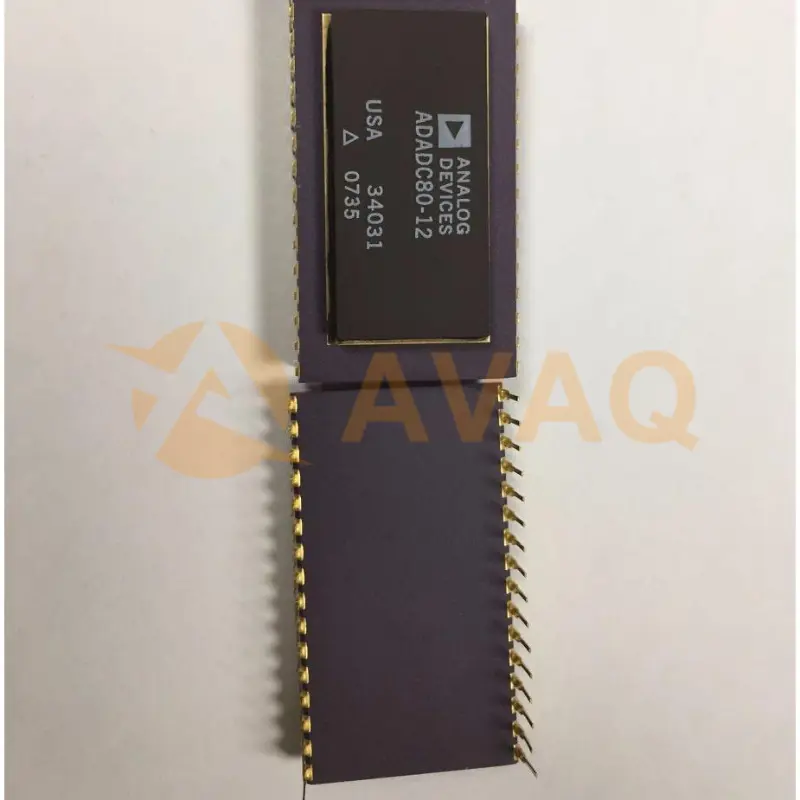
Dual Channel Single ADC SAR 12-bit Parallel 32-Pin SBCDIP
Manufacturer:
Mfr.Part #:
ADADC80-12
Datasheet:
Pbfree Code:
Yes
Part Life Cycle Code:
Obsolete
Pin Count:
32
HTS Code:
8542.39.00.01
EDA/CAD Models:
Please fill in the short form below and we will provide you the quotation immediately.
The ADADC80* is a complete 12-bit successive-approximation analog-to-digital converter (ADC) that includes an internal clock, reference, and comparator. Its hybrid IC design uses MSI digital and linear monolithic chips in conjunction with a 12-bit monolithic digital-to-analog converter (DAC) to provide modular performance and versatility with IC size, price, and reliability. Important performance characteristics of the ADADC80 include a maximum linearity error of ±0.012% at 25°C, maximum gain TC of 30 ppm/°C, typical power dissipation of 800 mW, and maximum conversion time of 25 µs. Monotonic operation of the feedback DAC guarantees no missing codes over the temperature range of -25°C to +85°C. The design of the ADADC80 includes scaling resistors that provide an analog signal range of ±2.5 V, ±5.0 V, ±10 V, 0 V to +5.0 V, or 0 V to +10.0 V. The 6.3 V precision reference can be used for external applications. All digital signals are fully DTL and TTL compatible; output data is in parallel form. The ADADC80 is available in grades specified for use over the -25°C to +85°C temperature range and is available in a 32-lead ceramic DIP. Product Highlights The ADADC80 is a complete 12-bit ADC. No external components are required to perform a conversion. A monolithic 12-bit feedback DAC is used for reduced chip count and higher reliability. The internal buried Zener reference is laser trimmed to 6.3 V. The reference voltage is available externally and can supply up to 1.5 mA beyond the current required for the reference and bipolar offset. The scaling resistors are included on the monolithic DAC for exceptional thermal tracking. The ADADC80 directly replaces other devices of this type, providing significant increases in performance. The fast conversion rate of the ADADC80 makes it an excellent choice for applications requiring high system throughput rates. The short cycle and external clock options are provided for applications requiring faster conversion speed or lower resolution. * The serial output function is no longer supported on this product after Date Code 9616. Data Sheet, Rev. E, 2/08
| Source Content uid | ADADC80-12 | Pbfree Code | Yes |
| Part Life Cycle Code | Obsolete | Pin Count | 32 |
| Reach Compliance Code | HTS Code | 8542.39.00.01 | |
| Analog Input Voltage-Max | 10 V | Analog Input Voltage-Min | -10 V |
| Conversion Time-Max | 25 µs | Converter Type | ADC, SUCCESSIVE APPROXIMATION |
| JESD-30 Code | R-CDIP-T32 | JESD-609 Code | e4 |
| Length | 30.48 mm | Linearity Error-Max (EL) | 0.012% |
| Negative Supply Voltage-Nom | -15 V | Number of Analog In Channels | 2 |
| Number of Bits | 12 | Number of Functions | 1 |
| Number of Terminals | 32 | Operating Temperature-Max | 85 °C |
| Operating Temperature-Min | -25 °C | Output Bit Code | COMPLEMENTARY BINARY, COMPLEMENTARY 2'S COMPLEMENT, COMPLEMENTARY OFFSET BINARY |
| Output Format | PARALLEL, WORD | Qualification Status | Not Qualified |
| Sample and Hold / Track and Hold | SAMPLE | Seated Height-Max | 7.11 mm |
| Supply Voltage-Nom | 15 V | Surface Mount | NO |
| Technology | HYBRID | Temperature Grade | OTHER |
| Terminal Finish | GOLD | Terminal Form | THROUGH-HOLE |
| Terminal Pitch | 2.54 mm | Terminal Position | DUAL |
| Width | 15.24 mm |
After-Sales & Settlement Related
 Payment
Payment Method


For alternative payment channels, please reach out to us at:
[email protected] Shipping & Packing
Shipping Method


AVAQ determines and packages all devices based on electrostatic discharge (ESD) and moisture sensitivity level (MSL) protection requirements.
 Warranty

365-Day Product
Quality Guarantee
We promise to provide 365 days quality assurance service for all our products.
| Qty. | Unit Price | Ext. Price |
|---|---|---|
| 1+ | - | - |
The prices below are for reference only.
All bill of materials (BOM) can be sent via email to ![]() [email protected],
or fill below form to Quote for ADADC80-12, guaranteed quotes back within
[email protected],
or fill below form to Quote for ADADC80-12, guaranteed quotes back within
![]() 12hr.
12hr.
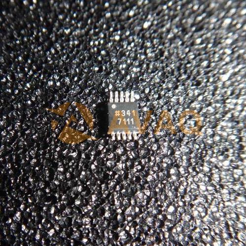
AD9833BRMZ
Analog Devices
100+ $4.303
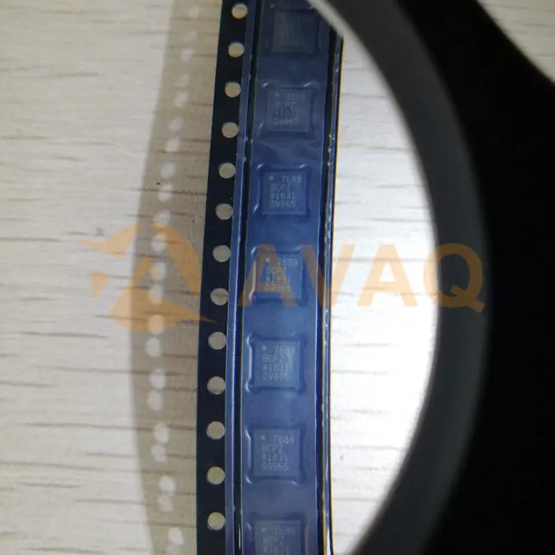
AD7689BCPZ
Analog Devices
100+ $4.118

AD9208
ADI
Analog to Digital Converters - ADC Eval Bd for AD9208-3000
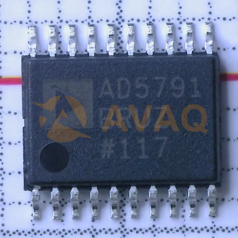
AD5791BRUZ
Analog Devices
With its segment design, the AD5791BRUZ ensures precise and stable analog output in a variety of industrial and instrumentation settings
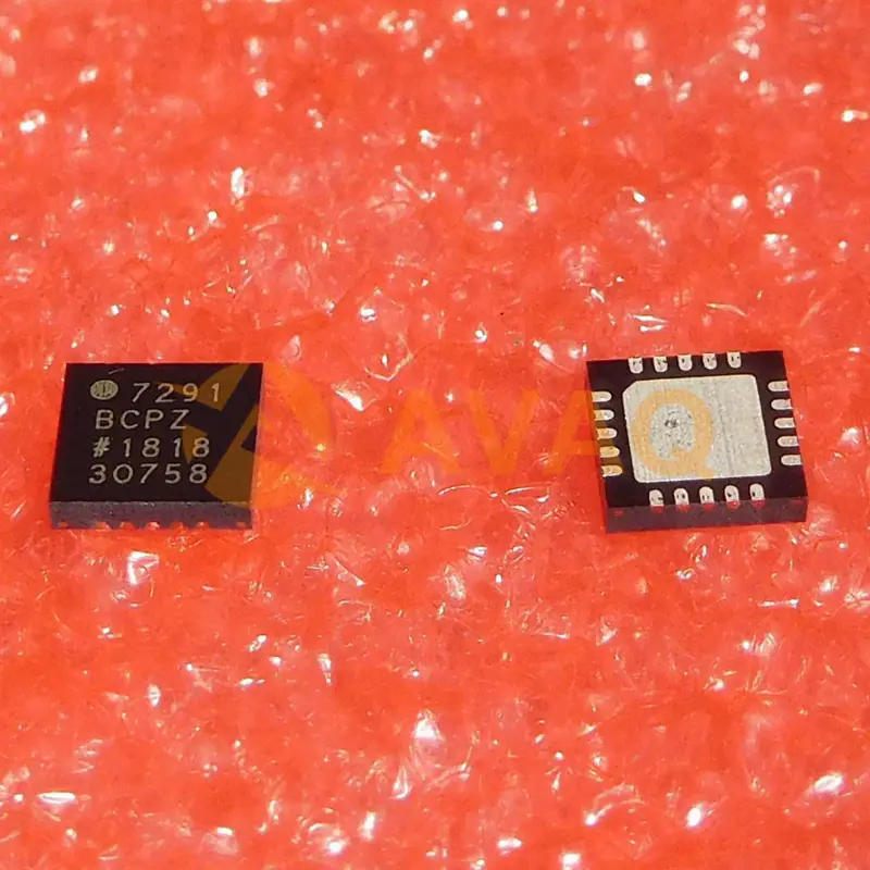
AD7291BCPZ
Analog Devices, Inc
8-Channel Single ADC SAR 22.22ksps 12-bit Serial 20-Pin LFCSP EP Tray
