What is QFP Package: Features, Types and Applications 2023
 Published: Oct 11, 2023
Contents
In the fast-paced world of integrated circuits and semiconductor devices, the packaging is often as critical as the technology it contains. One such packaging format that has become synonymous with compact, high-performance electronic components is the Quad Flat Package, or QFP.
In this article, we will explore the world of QFP packages, delving into their design, applications, and the pivotal role they play in modern electronics and technology.
What is the QFP Package?
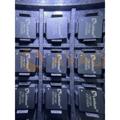
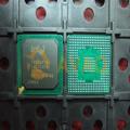
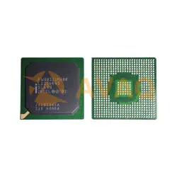
QFP stands for Quad Flat Package, and it is a type of surface-mount integrated circuit package used for electronic components such as microcontrollers, microprocessors, and other integrated circuits. The QFP package is characterized by its flat, square or rectangular shape with leads (pins) extending from all four sides of the package, forming a "quad" configuration. These leads are typically arranged in a grid pattern, which makes it easier to solder the component onto a printed circuit board (PCB).
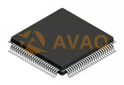
Quad Side Pin Flat Packages, commonly known as QFPs, are surface mount integrated circuit packages featuring pins extending from all four sides in a gullwing (L) shape. These packages are made from a variety of materials, including ceramic, metal, and plastic. Plastic QFPs are the most prevalent due to their affordability and adaptability. They are the preferred choice for numerous multi-pin LSI (Large Scale Integration) applications.
QFPs are utilized not only for digital logic LSI circuits such as microprocessors and gate arrays but also for analog LSI circuits like VTR (Video Tape Recorder) signal processing and audio signal processing. They come in a range of specifications, denoted by the center distance between pins, with options including 1.0mm, 0.8mm, 0.65mm, 0.5mm, 0.4mm, and 0.3mm. The maximum number of pins available in the 0.65mm center distance specification is 304.
QFPs with a pin center distance of less than 0.65mm are often referred to as QFPs (FPs) in Japan. However, the JAPON Electronic and Mechanical Industries Association has redefined QFP specifications based on package body thickness, categorizing them as QFP (2.0mm to 3.6mm thick), LQFP (1.4mm thick), and TQFP (1.0mm thick).
Some LSI manufacturers designate QFPs with a 0.5mm pin center distance as Shrinkable QFPs (SQFPs) or Very Thin QFPs (VQFPs). The nomenclature can be confusing, as some manufacturers also label QFPs with 0.65mm and 0.4mm pin center distances as SQFPs.
A drawback of QFPs with pin center distances less than 0.65mm is their susceptibility to pin bending. To address this issue, several improved QFP varieties have been introduced, including BQFPs with resin buffers, GQFPs with resin protective rings, and TPQFPs with test bumps for pin protection during testing.
For logic LSIs, many developmental and high-reliability products are packaged in multilayer ceramic QFPs. These products feature a minimum pin center distance of 0.4mm and can accommodate a maximum of 348 pins. Additionally, there are glass-sealed ceramic QFPs known as Cerquads. These packages offer various options for different applications and requirements within the realm of integrated circuits.
Different Types of QFP Packages -- Variants
QFP (Quad Flat Package) is a versatile surface mount integrated circuit package with various subtypes that differ primarily in lead counts, dimensions, and materials. Here are descriptions of some common QFP subtypes:
TQFP (Thin Quad Flat Package):
- Description: TQFP packages offer the same benefits as regular QFPs but are thinner. They are designed to address issues like increasing board density, die shrink programs, and achieving a thinner end-product profile.
- Thickness: TQFP packages range from 1mm to 1.4mm, which is notably thinner than standard QFP packages.
- Lead Count: Lead counts range from 32 to 176.
- Pins: Available with various lead pitches, such as 0.4 mm, 0.5 mm, 0.65 mm, 0.8 mm, and 1.0 mm.
LQFP (Low Profile Quad Flat Package):
- Description: LQFP is a surface mount IC package format with component leads extending from each of its four sides. It is known for its low profile.
- Lead Count: Varies according to the specific LQFP package.
- Pins: Available with different pin spacings, such as 0.4 mm, 0.5 mm, 0.65 mm, and 0.80 mm intervals.
PQFP (Plastic Quad Flat Package):
- Description: PQFP is a type of QFP, and it shares similarities with TQFP packages but with a broader thickness range.
- Thickness: PQFP packages can vary in thickness, typically ranging from 2.0 mm to 3.8 mm.
CQFP (Ceramic Quad Flat Package):
- Description: CQFP is a QFP package with a ceramic substrate, providing enhanced thermal characteristics and reliability.
- Material: The package body is made of ceramic, offering improved thermal performance.
These QFP variants offer flexibility in terms of package thickness, lead counts, and thermal characteristics, catering to diverse application requirements. Additionally, other QFP subtypes include BQFP (Bumpered Quad Flat Package), EQFP (Plastic Enhanced Quad Flat Package), FQFP (Fine Pitch Quad Flat Package), MQFP (Metric Quad Flat Package), NQFP (Near Chip-Scale Quad Flat Package), SQFP (Small Quad Flat Package), VQFP (Very Small Quad Flat Package), VTQFP (Very Thin Quad Flat Package), and TDFN (Thin Dual Flat No-Lead Package). Each subtype serves specific needs in the electronics industry, offering designers a wide range of options for integrated circuit packaging.
QFP Packages Process Flow
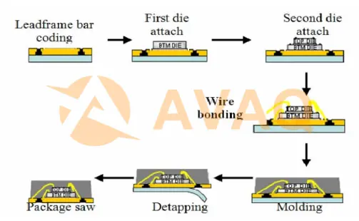
- Wafer Fabrication: Create integrated circuits on silicon wafers.
- Die Attach: Bond ICs to a substrate.
- Wire Bonding: Connect wires from ICs to leads.
- Mold Encapsulation: Protect ICs with plastic or ceramic.
- Testing: Verify IC performance.
- Lead Plating: Plate leads for solderability.
- Surface-Mount Assembly: Attach QFPs to PCB.
- Soldering: Secure connections with solder.
- Testing: Check PCB functionality.
- Packaging: Enclose PCB if needed.
- Quality Control: Ensure product meets standards.
- Shipping: Distribute final products to customers.
Features of QFP Package
- Compact Design: QFPs have a space-efficient square or rectangular shape with leads on all four sides.
- Variety of Sizes: QFP packages come in various sizes, lead counts, and lead pitches to accommodate different ICs.
- Surface Mount Technology (SMT): Designed for surface mount assembly, QFPs are compatible with modern PCB manufacturing processes.
- Good Thermal Performance: QFPs often have an exposed metal pad on the bottom, which aids in heat dissipation, suitable for ICs with thermal considerations.
- High Pin Density: QFPs can support a high number of pins, making them suitable for complex integrated circuits.
- Ease of Inspection: Leads on QFPs are visible for visual inspection and testing.
- Robust and Durable: QFPs are typically made from plastic or ceramic, providing protection and durability for encapsulated ICs.
- Versatility: QFPs are used for a wide range of ICs, including microcontrollers, microprocessors, memory chips, and other digital or analog devices.
- Solderability: QFP leads are often plated with materials like solder, simplifying the soldering process to the PCB.
- Compatibility: QFPs adhere to industry-standard sizes and dimensions, ensuring compatibility with various PCB designs and manufacturing processes.
- Cost-Effective: QFP packages are often cost-effective, especially in plastic variants, contributing to overall cost savings in electronic device manufacturing.
- Standardization: QFPs follow industry standards, simplifying the design and assembly process
Applications of QFP package
Here's a table outlining the applications, common models, manufacturers, and characteristics of QFP (Quad Flat Package) components,
|
Application Type |
Common Models |
Manufacturers |
Characteristics |
|
Microcontrollers and Microprocessors |
Microchip (formerly Atmel) |
Compact design, suitable for embedded systems and IoT devices. |
|
|
Digital Signal Processors (DSPs) |
ADSP-21469 |
Analog Devices |
Used for audio processing, image processing, and communication applications. |
|
Memory ICs |
S29GL512P11TFI01 |
Cypress Semiconductor |
Commonly used in smartphones, tablets, and storage devices. |
|
Application-Specific Integrated Circuits (ASICs) |
LatticeXP2 |
Lattice Semiconductor |
Used for specific applications and custom logic with flexibility. |
|
PCB Components |
Various |
Multiple Manufacturers |
Provides integrated circuit solutions for control, interfaces, and other functions on PCBs. |
|
Consumer Electronics |
Microchip (formerly Atmel) |
Used in devices like TVs, set-top boxes, gaming consoles, and home appliances. |
|
|
Communication Devices |
MT7621 |
MediaTek |
Suitable for routers, switches, and network interface cards, among others. |
|
Automotive Electronics |
Freescale MC9S12XDP512 |
NXP Semiconductors |
Used in engine control units (ECUs), infotainment systems, and safety systems. |
|
Industrial Control Systems |
STM32F4xx |
STMicroelectronics |
Applied in industrial automation, PLCs (Programmable Logic Controllers), and robot control. |
|
Medical Devices |
MSP430FR5994 |
Texas Instruments |
Used in diagnostic equipment and patient monitors, known for low power and reliability. |
|
Aerospace and Defense |
FPGAs: Xilinx Virtex Series |
Xilinx, Inc. |
Employed in aerospace electronic systems, radar equipment, and military applications for high performance and programmability. |
|
Networking Equipment |
Cisco 4000 Series Routers |
Cisco Systems, Inc. |
Used in network routers and switches, supporting high-speed data transmission. |
|
Measurement and Testing Instruments |
Tektronix TBS1000 Series Oscilloscopes |
Tektronix, Inc. |
Applied in oscilloscopes, spectrum analyzers, and other measurement equipment with data processing capabilities. |
|
Gaming Devices |
AMD Ryzen Processors |
Advanced Micro Devices (AMD) |
Used in gaming consoles and handheld gaming devices, providing graphics processing and system control. |
|
Security Systems |
DS28E80 |
Maxim Integrated |
Used in security cameras, access control systems, and alarm systems, offering data processing capabilities. |
|
Smartphones and Tablets |
Snapdragon Processors |
Qualcomm |
Employed in mobile devices for processing, wireless communication, and multimedia capabilities. |
Advantages and Disadvantages of QFP Packages
Here are the primary advantages and disadvantages of QFP packages:
Advantages of QFP Packages:
- Compact Design: QFP packages have a space-efficient, flat design, which helps save space on printed circuit boards (PCBs).
- High Pin Density: They can accommodate a high number of pins, making them suitable for complex integrated circuits.
- Ease of Inspection: The leads on QFPs are easily visible, allowing for visual inspection and testing.
- Surface Mount Technology (SMT): QFPs are designed for surface mount assembly, making them compatible with modern PCB manufacturing techniques and automated assembly processes.
- Thermal Performance: The exposed metal pad on the bottom of QFP packages enhances heat dissipation, making them suitable for ICs with thermal considerations.
- Versatility: QFP packages are used in a wide range of applications, including microcontrollers, microprocessors, memory chips, and other digital or analog devices.
- Standardization: QFP packages adhere to industry-standard sizes and dimensions, simplifying the design and assembly process.
- Cost-Effective: QFP packages are often cost-effective, especially in plastic variants, contributing to overall cost savings in electronic device manufacturing.
- Robust and Durable: QFP packages are typically made from plastic or ceramic materials, providing protection and durability for encapsulated ICs.
Disadvantages of QFP Packages:
- Lead Bending: The leads of QFP packages can be more susceptible to bending during handling or assembly, requiring careful handling.
- Limited Heat Dissipation: While QFPs have good thermal properties, they may not be as effective as other packages, such as ceramic, in managing very high heat loads.
- Rework Difficulty: Repairing or replacing QFP components can be challenging, as de-soldering and re-soldering requires specialized equipment and skills.
- Risk of Solder Bridging: During soldering, there's a potential risk of solder bridging between closely spaced leads, which can affect functionality.
- Not Ideal for High-Frequency Applications: For very high-frequency applications, QFP packages may not be as suitable as packages designed for better high-frequency performance.
- Limited to Surface Mount: QFPs are designed for surface mounting, so they may not be suitable for applications that require through-hole components.
- Size Limitations: While available in various sizes, very large or very small ICs may not be well-suited to QFP packages, which can limit their use in extreme size cases.
- Risk of Lead Damage: The exposed leads of QFPs are susceptible to physical damage if not handled carefully.
Differences between QFP and QFN Packages
QFP packages and QFN (Quad Flat No-leads) packages are two common surface mount package technologies that have a number of differences, including the following:
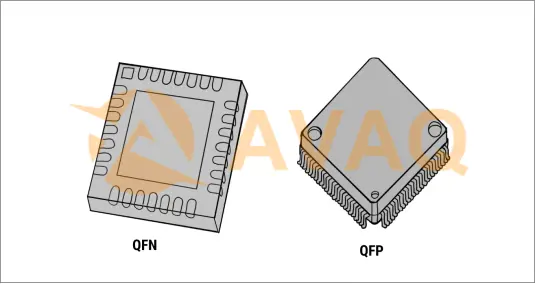
1. ☞Pin Layout: The pins of a QFP package are located on all four sides of the package and are usually arranged at right angles. QFN packages have pins located on the bottom of the package and are usually aligned with the edges of the chip.
2. ☞Pin type: QFP package pins are visible metal pins that can be used for soldering and connecting. QFN package pins are usually hidden at the bottom of the package, through the bottom of the package metal pads to achieve soldering and connection.
3. ☞Pin spacing: Usually, the pin spacing of the QFP package is small, the common spacing including 0.5mm, 0.4mm, etc. The QFN package is usually hidden at the bottom of the package. QFN package pin spacing is usually larger, the common pitch including 0.65mm, 0.8mm, etc.
4. ☞Size and number of pins: QFP packages usually have a larger size and a larger number of pins, for applications requiring high pin density. QFN package usually has a smaller size and less number of pins, suitable for applications with more stringent size requirements.
5. ☞Thermal performance: Since the pins of the OFN package are located on the bottom metal coal pan, the thermal conductivity with the PCB is better, which helps to improve the heat dissipation ability.
It should be noted that although the QFP and QFN packages in some aspects of the obvious differences, but they also have some common points, such as surface mount technology, high pin density, miniaturized design. When selecting a package form, comprehensive consideration should be made based on specific application needs and design requirements.
Conclusion
In conclusion, the QFP package has left an indelible mark on the electronics industry, and its significance continues to grow as technology advances. The combination of a small form factor, high pin count, and efficient heat dissipation makes it a popular choice for various applications, from consumer electronics to industrial control systems.
Next Industry Focus
The Ultimate Guide to Power Management Integrated Circuits 2023
 Update Time: Oct 16, 2023 Consumer Electronics
 FAQ
FAQ
- Are there alternatives to QFP packages?
- Yes, there are various IC package types, such as Ball Grid Array (BGA), Chip-On-Board (COB), and Small Outline Integrated Circuit (SOIC) packages, which offer different form factors and characteristics to suit specific application requirements.
- What challenges are associated with QFP packages?
- Smaller Pitch: As pin counts increase, the distance between pins (pitch) becomes smaller, requiring precision during soldering and rework. Inspection: Inspection of solder joints can be challenging due to the fine pitch, requiring magnification and possibly X-ray inspection. Rework: Reworking QFP packages can be difficult, especially if a solder joint needs to be corrected or a component needs to be replaced.
- How do you solder QFP packages to a PCB?
- QFP packages are soldered to a printed circuit board (PCB) using surface-mount technology (SMT). The process typically involves applying solder paste to the PCB pads, placing the QFP component on the pads, and then using a reflow soldering process to melt the solder and create a secure connection between the component and the PCB.
Related Industry Focus
-
![Nuvoton NCT6791D: Datasheet, Features and Applications]()
Nuvoton NCT6791D: Datasheet, Features and Applications
From temperature and voltage monitoring to fan control and system interactivity, the Nuvoton NCT6791D is a critical component in modern computer motherboards. In this article, we will delve into the Datasheet, Features, and Applications of the Nuvoton NCT6791D, shedding...
Published: 2023-10-09 16:50:32 -
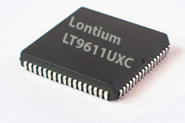
![LT9611UXC Lontium: Datasheet, Features and Applications]()
LT9611UXC Lontium: Datasheet, Features and Applications
The LT9611UXC is a multimedia converter chip manufactured by Lontium Semiconductor Corporation. It is designed to convert MIPI DSI (Display Serial Interface) and CSI (Camera Serial Interface) signals to HDMI 2.0 output. This makes it a valuable component for connecting ...
Published: 2023-09-27 16:19:44 -
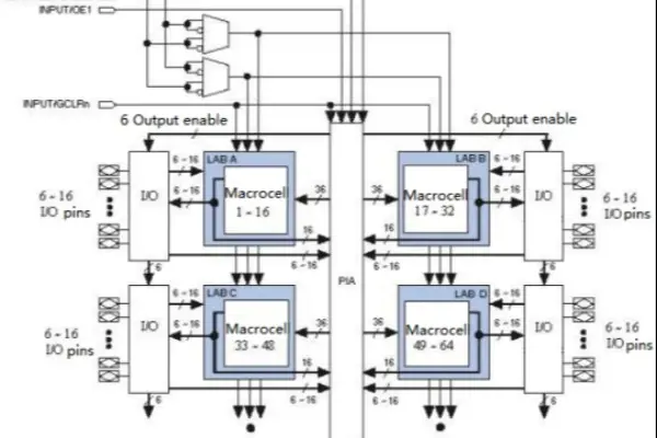
![What is Complex Programmable Logic Device(CPLD)]()
What is Complex Programmable Logic Device(CPLD)
Complex Programmable Logic Devices (CPLDs) are digital integrated circuits with programmable logic cells and interconnections used to implement a variety of digital logic functions for a wide range of applications, including system control, signal processing, and interf...
Published: 2023-09-25 17:49:42 -
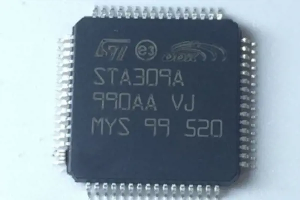
![STA309A Digital Audio Processor DDX: Datasheet, Pinout and Application]()
STA309A Digital Audio Processor DDX: Datasheet, Pinout and Application
The STA309A is a multi-channel digital audio processor developed by STMicroelectronics, featuring 8 channels of 24-bit DDX® technology. In this comprehensive guide, we will delve into the Datasheet, Pinout, and Application of the STA309A Digital Audio Processor DDX, ex...
Published: 2023-09-22 16:01:57
PIC16F877A-I/P In Stock: 6976 $3.408
 Popular Industry Focus
Hot Products
-
![AT24C08BN-SH-T]()
AT24C08BN-SH-T
MICROCHIP
EEPROM Memory IC 8Kbit I2C 1 MHz 550 ns 8-SOIC
-
![AT90S4433-8AI]()
AT90S4433-8AI
Microchip
AT90S4433-8AI by Microchip Technology
-
![ATMEGA64-16AU]()
ATMEGA64-16AU
Microchip
AVR microcontroller
-
![2N3879]()
2N3879
Microchip
Bipolar (BJT) Transistor NPN 75 V 7 A 35 W Through Hole TO-66 (TO-213AA)
-
![ATMEGA8A-PU]()
ATMEGA8A-PU
MICROCHIP
Microcontroller 8-bit AVR
-
![MCP4726A0T-E/MAY]()
MCP4726A0T-E/MAY
MICROCHIP
12-Bit Single Output DAC w/EEPROM and I2C™.


Related Parts
-
![AD8030ARZ]()
AD8030ARZ
Analog Devices Inc.
General Purpose Amplifier 2 Circuit Rail-to-Rail 8-SOIC
-
![AM79C874VI]()
AM79C874VI
Amd
High-speed communication solution for Ethernet connectivity with versatile 3.3V support and space-saving 80-pin TQFP form factor
-
![TMPZ84C015BF-12]()
TMPZ84C015BF-12
TOSHIBA CORP
IC MICROPROCESSOR, PQFP100, PLASTIC, QFP-100, Microprocessor
-
![CLOM8214]()
CLOM8214
QLOGIC CORP
Micro Peripheral IC,
-
![ASM1442]()
ASM1442
Asmedia Technology Inc
Consumer Circuit, ROHS COMPLIANT, QFN-48
-
![AIC-7892B]()
AIC-7892B
ADAPTEC
-
![CH7026B-TF]()
CH7026B-TF
CHRONTEL INC
TV/VGA Encoder, LQFP-80
-
![K9F1G08U0A-PCB0]()
K9F1G08U0A-PCB0
SAMSUNG
Flash, 128MX8, 20ns, PDSO48
-
![LT9611UXC]()
LT9611UXC
Lontium Semiconductor Corporation
Multimedia Converter MIPI DSI/CSI to HDMI2.0 6Gbps 64-Pin QFN
-
![NH82801DB SL8DE]()
NH82801DB SL8DE
Intel Corp
I/O Controller 421-Pin BGA
-
![FW82801BA]()
FW82801BA
Intel
Intel® 82801FB I/O Controller Hub ICH6
-
![NHE6300ESB]()
NHE6300ESB
INTEL
IO Controller Hub, NHE6300ESB
-
![PCF7953PTTM1AC1800]()
PCF7953PTTM1AC1800
NXP USA Inc.
RF Transmitter Antenna 28-TSSOP (0.173", 4.40mm Width)
-
![XB3-24Z8US]()
XB3-24Z8US
Digi
Zigbee Modules - 802.15.4 XBee3 PRO,2.4 Ghz ZB 3.0, U.FL Ant, SMT
-
![WT12-A-AI4]()
WT12-A-AI4
Silicon Labs
Bluetooth Bluetooth v2.1 +EDR, Class 2 Transceiver Module 2.4GHz Integrated, Chip Surface Mount


Featured Manufacturers