This website uses cookies. By using this site, you consent to the use of cookies. For more information, please take a look at our Privacy Policy.

TPS54116QRTWRQ1

- Converter, DDR Voltage Regulator IC 1 Output 24-WQFN (4x4)

TPS54116QRTWRQ1 General Description

The TPS54116-Q1 device is a full featured 6-V, 4-A, synchronous step down converter with two integrated MOSFETs and 1-A sink/source double data rate (DDR) VTT termination regulator with VTTREF buffered reference output.

The TPS54116-Q1 buck regulator minimizes solution size by integrating the MOSFETs and reducing inductor size with up to 2.5-MHz switching frequency. The switching frequency can be set above the medium wave radio band for noise sensitive applications and is synchronizable to an external clock. Synchronous rectification keeps the frequency fixed across the entire output load range. Efficiency is maximized through integrated 25-mΩ low-side and 33-mΩ high-side MOSFETs. Cycle-by-cycle peak current limit protects the device during an overcurrent condition and is adjustable with a resistor at the ILIM pin to optimize for smaller inductors.

The VTT termination regulator maintains fast transient response with only 2 × 10-µF ceramic output capacitance reducing external component count. The TPS54116-Q1 uses remote sensing of VTT for best regulation.

Using the enable pins to enter a shutdown mode reduces supply current to 1-µA. Under voltage lockout thresholds can be set with a resistor network on either enable pin. The VTT and VTTREF outputs are discharged when disabled with ENLDO.

Full integration minimizes the IC footprint with a small 4 mm × 4 mm thermally enhanced WQFN package.

TPS54116QRTWRQ1 TPS54116QRTWRQ1

Key Features

  • AEC-Q100 Qualified With the Following Results:
    • Device Temperature Grade 1: –40°C to +125°C Ambient Operating Temperature Range
    • Device HBM ESD Classification Level 2
    • Device CDM ESD Classification Level C6
  • Single-chip DDR2, DDR3 and DDR3L Memory Power Solution
  • 4-A Synchronous Buck Converter
    • Integrated 33-mΩ High-side and 25-mΩ Low-side MOSFETs
    • Fixed Frequency Current-mode Control
    • Adjustable Frequency from 100 kHz to 2.5 MHz
    • Synchronizable to an External Clock
    • 0.6-V ±1% Voltage Reference Over Temperature
    • Adjustable Cycle-by-Cycle Peak Current Limit
    • Monotonic Start-up Into Pre-biased Outputs
  • 1-A Source/Sink Termination LDO with ±20-mV DC Accuracy
    • Stable with 2 × 10-µF MLCC Capacitor
    • 10-mA Source/Sink Buffered Reference Output Regulated to Within 49% to 51% of VDDQ
  • Independent Enable Pins with Adjustable UVLO and Hysteresis
  • Thermal Shutdown
  • –40°C to 150°C Operating TJ
  • 24-pin, 4-mm × 4-mm WQFN Package

Specifications

Vin (min) (V) 2.95 Vin (max) (V) 6
Rating Automotive Iq (typ) (mA) 0.65
Features Complete Solution, Power good, Shutdown Pin for S3 Operating temperature range (°C) -40 to 125

Service Policies and Others

After-Sales & Settlement Related

payment Payment

Payment Method

hsbc
TT/Wire Transfer
paypal
Paypal
wu
Western Union
mg
Money Gram

For alternative payment channels, please reach out to us at:

[email protected]
shipping Shipping & Packing

Shipping Method

fedex
Fedex
ups
UPS
dhl
DHL
tnt
NTN
Packing

AVAQ determines and packages all devices based on electrostatic discharge (ESD) and moisture sensitivity level (MSL) protection requirements.

Warranty Warranty

We promise to provide 365 days quality assurance service for all our products.

Ratings and Reviews

More
Z
Z**y 07/23/2022

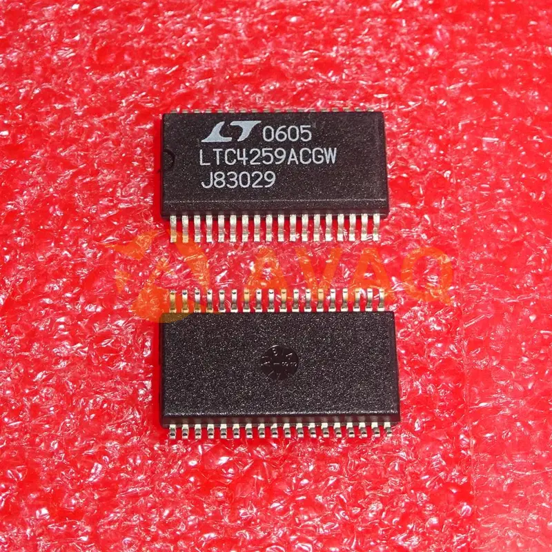
Long went. Everything came in intact. On windows 10 is defined.

2

Reviews

You need to log in to reply. Sign In | Sign Up

Availability: 4744 PCS

+BOM
Qty. Unit Price Ext. Price
1+ - -

The prices below are for reference only.