Payment Method


Enhanced product LVDS SerDes transmitter
Manufacturer:
Mfr.Part #:
SN65LVDS95DGGREP
Datasheet:
Function:
Serializer
Data Rate:
1.3Gbps
Input Type:
LVDS
Output Type:
LVTTL
EDA/CAD Models:
Please fill in the short form below and we will provide you the quotation immediately.
The SN65LVDS95 LVDS serdes (serializer/deserializer) transmitter contains three 7-bit parallel-load serial-out shift registers, a 7× clock synthesizer, and four low-voltage differential signaling (LVDS) line drivers in a single integrated circuit. These functions allow 21 bits of single-ended LVTTL data to be synchronously transmitted over 4 balanced-pair conductors for receipt by a compatible receiver, such as the SN65LVDS96.
When transmitting, data bits D0 through D20 are each loaded into registers of the SN65LVDS95 on the rising edge of the input clock signal (CLKIN). The frequency of CLKIN is multiplied seven times and then used to serially unload the data registers in 7-bit slices. The three serial streams and a phase-locked clock (CLKOUT) are then output to LVDS output drivers. The frequency of CLKOUT is the same as the input clock, CLKIN.
The SN65LVDS95 requires no external components and little or no control. The data bus appears the same at the input to the transmitter and output of the receiver with data transmission transparent to the user(s). The only user intervention is the possible use of the shutdown/clear (SHTDN) active-low input to inhibit the clock and shut off the LVDS output drivers for lower power consumption. A low level on this signal clears all internal registers to a low level.
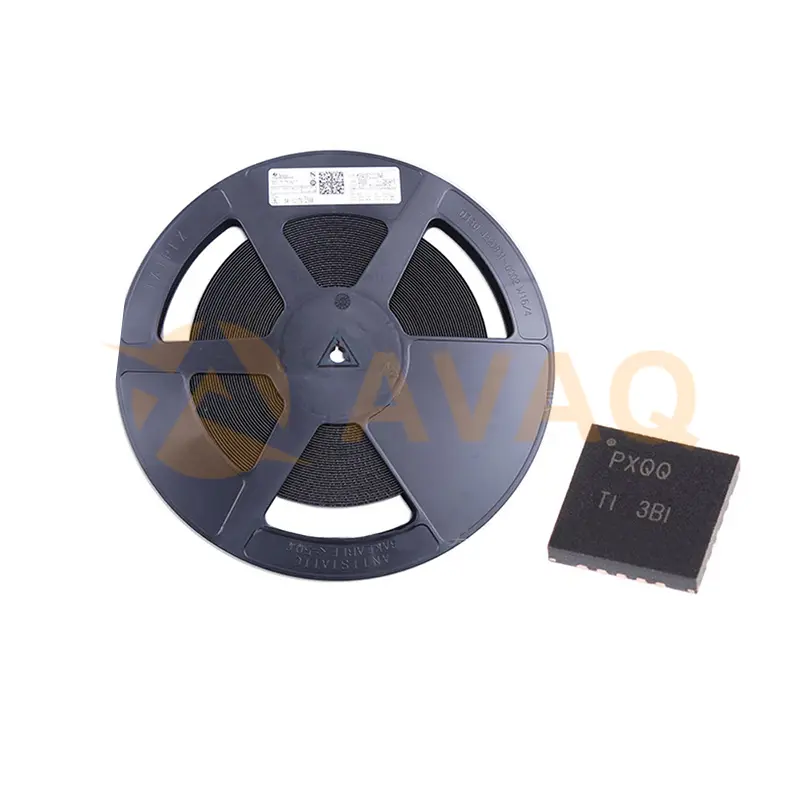
Component qualification in accordance with JEDEC and industry standards to ensure reliable operation over an extended temperature range. This includes, but is not limited to, Highly Accelerated Stress Test (HAST) or biased 85/85, temperature cycle, autoclave or unbiased HAST, electromigration, bond intermetallic life, and mold compound life. Such qualification testing should not be viewed as justifying use of this component beyond specified performance and environmental limits.
| Category | Integrated Circuits (ICs)InterfaceSerializers, Deserializers | Series | - |
| Function | Serializer | Data Rate | 1.3Gbps |
| Input Type | LVDS | Output Type | LVTTL |
| Number of Inputs | 21 | Number of Outputs | 3 |
| Voltage - Supply | 3V ~ 3.6V | Operating Temperature | -40°C ~ 85°C (TA) |
| Mounting Type | Surface Mount | Base Product Number | 65LVDS95 |
| Protocols | HiRel Enhanced Product | Rating | HiRel Enhanced Product |
| Operating temperature range (°C) | -40 to 85 | feature-function | Serializer/Deserializer |
| feature-number-of-drivers | 3 | feature-number-of-receivers | 21 |
| feature-number-of-elements-per-chip | 3 | feature-transmission-data-rate-mbps | 1360 |
| feature-maximum-propagation-delay-time-ns | feature-input-signal-type | LVTTL | |
| feature-differential-input-low-threshold-voltage-v | feature-differential-input-high-threshold-voltage-v | ||
| feature-maximum-differential-output-voltage-v | 0.454 | feature-maximum-input-current-ua | |
| feature-supplier-temperature-grade | Industrial | feature-packaging | Tape and Reel |
| feature-rad-hard | feature-pin-count | 48 | |
| feature-cecc-qualified | No | feature-esd-protection | |
| feature-escc-qualified | feature-military | No | |
| feature-aec-qualified | No | feature-aec-qualified-number | |
| feature-auto-motive | No | feature-p-pap | No |
| feature-eccn-code | EAR99 | feature-svhc | Yes |
| feature-svhc-exceeds-threshold | No |
After-Sales & Settlement Related
 Payment
Payment Method


For alternative payment channels, please reach out to us at:
[email protected] Shipping & Packing
Shipping Method


AVAQ determines and packages all devices based on electrostatic discharge (ESD) and moisture sensitivity level (MSL) protection requirements.
 Warranty

365-Day Product
Quality Guarantee
We promise to provide 365 days quality assurance service for all our products.
| Qty. | Unit Price | Ext. Price |
|---|---|---|
| 1+ | $19.130 | $19.13 |
| 30+ | $18.335 | $550.05 |
The prices below are for reference only.
All bill of materials (BOM) can be sent via email to ![]() [email protected],
or fill below form to Quote for SN65LVDS95DGGREP, guaranteed quotes back within
[email protected],
or fill below form to Quote for SN65LVDS95DGGREP, guaranteed quotes back within
![]() 12hr.
12hr.
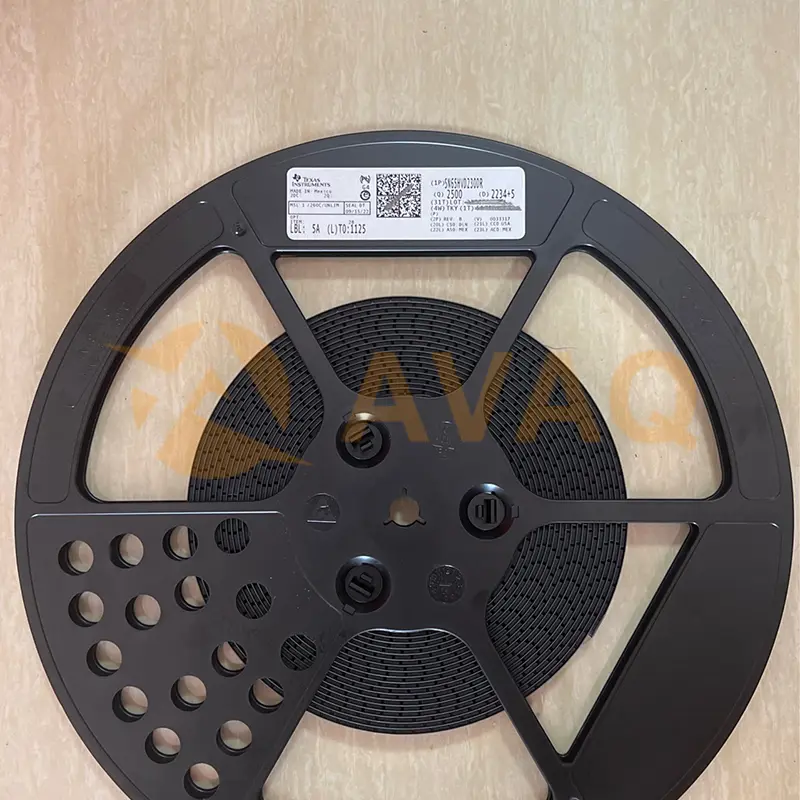
SN65HVD230DR
TI
1000+ $0.403
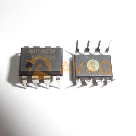
SN75176BP
TI
1000+ $0.309

PCF8574AN
TI
8-bit 2.5- to 5.5-V I2C/SMBus I/O expander with interrupt
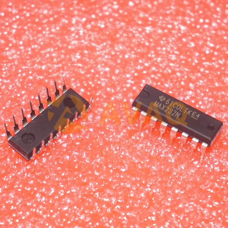
MAX232N
Texas Instruments, Inc
2/2 Transceiver Full RS232 16-PDIP
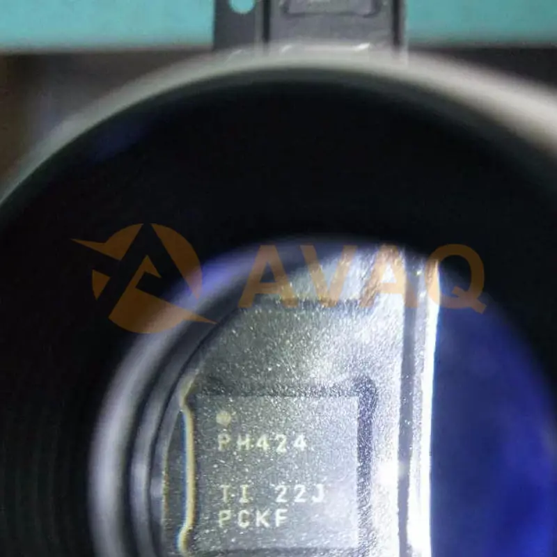
TCA6424RGJR
Texas Instruments, Inc
24-bit translating 1.65- to 5.5-V I2C/SMBus I/O expander with interrupt, reset & config registers