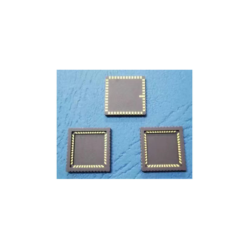
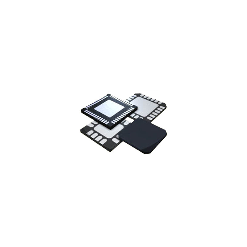
PCA9517DR General Description
This dual bidirectional I2C buffer is operational at 2.7 V to 5.5 V.
The PCA9517 is a BiCMOS integrated circuit intended for I2C bus and SMBus systems. It can also provide bidirectional voltage-level translation (up-translation/down-translation) between low voltages (down to 0.9 V) and higher voltages (2.7 V to 5.5 V) in mixed-mode applications. This device enables I2C and similar bus systems to be extended, without degradation of performance even during level shifting.
The PCA9517 buffers both the serial data (SDA) and the serial clock (SCL) signals on the I2C bus, thus allowing two buses of 400-pF bus capacitance to be connected in an I2C application. This device can also be used to isolate two halves of a bus for voltage and capacitance.
The PCA9517 has two types of drivers—A-side drivers and B-side drivers. All inputs and I/Os are overvoltage tolerant to 5.5 V, even when the device is unpowered (VCCB and/or VCCA = 0 V).
The PCA9517 doesnot support clock stretching and arbitration across the repeater.
The B-side drivers operate from 2.7 V to 5.5 V and behave like the drivers in the PCA9515A. The output low level for this internal buffer is approximately 0.5 V, but the input voltage must be 70 mV or more below the output low level when the output internally is driven low. The higher-voltage low signal is called a buffered low. When the B-side I/O is driven low internally, the low is not recognized as a low by the input. This feature prevents a lockup condition from occurring when the input low condition is released.
This type of design on the B side prevents it from being used in series with the PCA9515A and another PCA9517 (B side). This is because these devices do not recognize buffered low signals as a valid low and do not propagate it as a buffered low again.
The A-side drivers operate from 0.9 V to 5.5 V and drive more current. They do not require the buffered low feature (or the static offset voltage). This means that a low signal on the B side translates to a nearly 0-V low on the A side, which accommodates smaller voltage swings of lower-voltage logic. The output pulldown on the A side drives a hard low, and the input level is set at 0.3 VCCA to accommodate the need for a lower low level in systems where the low-voltage-side supply voltage is as low as 0.9 V.
The A side of two or more PCA9517s can be connected together to allow a star topography, with the A side on the common bus. Also, the A side can be connected directly to any other buffer with static- or dynamic-offset voltage. Multiple PCA9517s can be connected in series, A side to B side, with no buildup in offset voltage and with only time-of-flight delays to consider.
The PCA9517 drivers are enabled when VCCA is above 0.8 V and VCCB is above 2.5 V.
The PCA9517 has an active-high enable (EN) input with an internal pullup to VCCB, which allows the user to select when the repeater is active. This can be used to isolate a badly behaved slave on power-up reset. It should never change state during an I2C operation, because disabling during a bus operation hangs the bus, and enabling part way through a bus cycle could confuse the I2C parts being enabled. The EN input should change state only when the global bus and repeater port are in an idle state, to prevent system failures.
The PCA9517 includes a power-up circuit that keeps the output drivers turned off until VCCB is above 2.5 V and the VCCA is above 0.8 V. VCCB and VCCA can be applied in any sequence at power up. After power up and with the EN high, a low level on the A side (below 0.3 VCCA) turns the corresponding B-side driver (either SDA or SCL) on and drives the B side down to approximately 0.5 V. When the A side rises above 0.3 VCCA, the B-side pulldown driver is turned off and the external pullup resistor pulls the pin high. When the B side falls first and goes below 0.3 VCCB, the A-side driver is turned on and the A side pulls down to 0 V. The B-side pulldown is not enabled unless the B-side voltage goes below 0.4 V. If the B-side low voltage does not go below 0.5 V, the A-side driver turns off when the B-side voltage is above 0.7 VCCB. If the B-side low voltage goes below 0.4 V, the B-side pulldown driver is enabled, and the B side is able to rise to only 0.5 V until the A side rises above 0.3 VCCA. Then the B side continues to rise, being pulled up by the external pullup resistor. VCCA is only used to provide the 0.3 VCCA reference to the A-side input comparators and for the power-good-detect circuit. The PCA9517 logic and all I/Os are powered by the VCCB pin.
As with the standard I2C system, pullup resistors are required to provide the logic-high levels on the buffered bus. The PCA9517 has standard open-collector configuration of the I2C bus. The size of these pullup resistors depends on the system, but each side of the repeater must have a pullup resistor. The device is designed to work with Standard mode and Fast mode I2C devices in addition to SMBus devices. Standard mode I2C devices only specify 3 mA in a generic I2C system, where Standard mode devices and multiple masters are possible. Under certain conditions, higher termination currents can be used.

 Payment


 Shipping & Packing


 Warranty

As in the description. I recommend.