This website uses cookies. By using this site, you consent to the use of cookies. For more information, please take a look at our Privacy Policy.

OMAPL137BPTPH

ARM926EJ-S Microprocessor IC OMAP-L1x 1 Core, 32-Bit 300MHz 176-HLQFP (24x24)

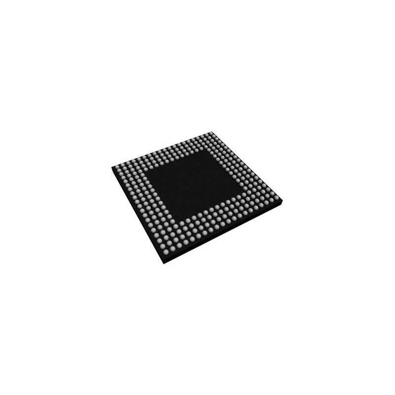
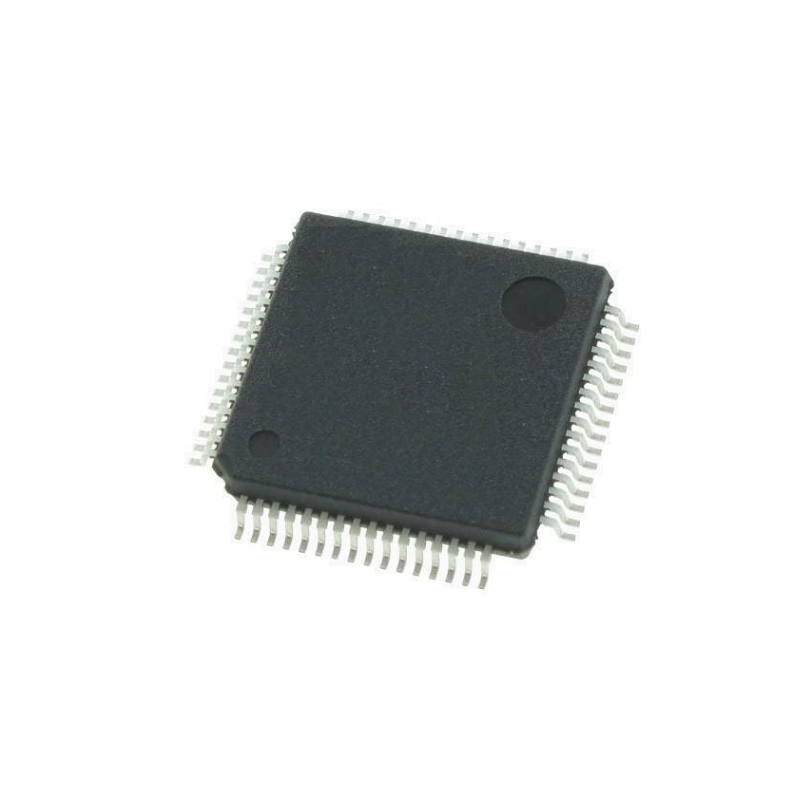
OMAPL137BPTPH General Description

The OMAPL137 is a low-power applications processor based on an ARM926EJ-S and a C674x DSP core. It consumes significantly lower power than other members of the TMS320C6000 platform of DSPs.

The OMAPL137 enables OEMs and ODMs to quickly bring to market devices featuring robust operating systems support, rich user interfaces, and high processing performance life through the maximum flexibility of a fully integrated mixed processor solution.

The dual-core architecture of the OMAPL137 provides benefits of both DSP and Reduced Instruction Set Computer (RISC) technologies, incorporating a high-performance TMS320C674x DSP core and an ARM926EJ-S core.

The ARM926EJ-S is a 32-bit RISC processor core that performs 32-bit or 16-bit instructions and processes 32-bit, 16-bit, or 8-bit data. The core uses pipelining so that all parts of the processor and memory system can operate continuously.

The ARM core has a coprocessor 15 (CP15), protection module, and Data and program Memory Management Units (MMUs) with table look-aside buffers. It has separate 16K-byte instruction and 16Kbyte data caches. Both are four-way associative with virtual index virtual tag (VIVT). The ARM core also has a 8KB RAM (Vector Table) and 64KB ROM.

The OMAPL137 DSP core uses a two-level cache-based architecture. The Level 1 program cache (L1P) is a 32KB direct mapped cache and the Level 1 data cache (L1D) is a 32KB 2-way set-associative cache. The Level 2 program cache (L2P) consists of a 256KB memory space that is shared between program and data space. L2 memory can be configured as mapped memory, cache, or combinations of the two. Although the DSP L2 is accessible by ARM and other hosts in the system, an additional 128KB RAM shared memory is available for use by other hosts without affecting DSP performance.

The peripheral set includes: a 10/100 Mb/s Ethernet MAC (EMAC) with a Management Data Input/Output (MDIO) module; two inter-integrated circuit (I2C) bus interfaces; 3 multichannel audio serial ports (McASP) with 16/12/4 serializers and FIFO buffers; 2 64-bit general-purpose timers each configurable (one configurable as watchdog); a configurable 16-bit host port interface (HPI) ; up to 8 banks of 16 pins of general-purpose input/output (GPIO) with programmable interrupt/event generation modes, multiplexed with other peripherals; 3 UART interfaces (one with RTS and CTS); 3 enhanced high-resolution pulse width modulator (eHRPWM) peripherals; 3 32-bit enhanced capture (eCAP) module peripherals which can be configured as 3 capture inputs or 3 auxiliary pulse width modulator (APWM) outputs; 2 32-bit enhanced quadrature pulse (eQEP) peripherals; and 2 external memory interfaces: an asynchronous and SDRAM external memory interface (EMIFA) for slower memories or peripherals, and a higher speed memory interface (EMIFB) for SDRAM.

The Ethernet Media Access Controller (EMAC) provides an efficient interface between the OMAP-L137 and the network. The EMAC supports both 10Base-T and 100Base-TX, or 10 Mbits/second (Mbps) and 100 Mbps in either half- or full-duplex mode. Additionally an Management Data Input/Output (MDIO) interface is available for PHY configuration.

The HPI, I2C, SPI, USB1.1 and USB2.0 ports allow the device to easily control peripheral devices and/or communicate with host processors.

The rich peripheral set provides the ability to control external peripheral devices and communicate with external processors. For details on each of the peripherals, see the related sections later in this document and the associated peripheral reference guides.

The device has a complete set of development tools for both the ARM and DSP. These include C compilers, a DSP assembly optimizer to simplify programming and scheduling, and a Windows® debugger interface for visibility into source code execution.

Texas Instruments, Inc Inventory

Key Features

  • Highlights
    • Dual Core SoC300-MHz ARM926EJ-S RISC MPU300-MHz C674x™ VLIW DSP
    • TMS320C674x Fixed/Floating-Point VLIW DSP Core
    • Enhanced Direct-Memory-Access Controller 3 (EDMA3)
    • 128K-Byte RAM Shared Memory
    • Two External Memory Interfaces
    • Two External Memory Interfaces Modules
    • LCD Controller
    • Two Serial Peripheral Interfaces (SPI)
    • Multimedia Card (MMC)/Secure Digital (SD)
    • Two Master/Slave Inter-Integrated Circuit
    • One Host-Port Interface (HPI)
    • USB 1.1 OHCI (Host) With Integrated PHY (USB1)
  • Applications
    • Industrial Diagnostics
    • Test and measurement
    • Military Sonar/Radar
    • Medical measurement
    • Professional Audio
    • Down Hole Industry
  • Software Support
    • TI DSP/BIOS
    • Chip Support Library and DSP Library
  • ARM926EJ-S Core
    • 32-Bit and 16-Bit (Thumb®) Instructions
    • DSP Instruction Extensions
    • Single Cycle MAC
    • ARM Jazelle Technology
    • EmbeddedICE-RT for Real-Time Debug
  • ARM9 Memory Architecture
  • C674x Instruction Set Features
    • Superset of the C67x+ and C64x+ ISAs
    • Up to 3648/2736 C674x MIPS/MFLOPS
    • Byte-Addressable (8-/16-/32-/64-Bit Data)
    • 8-Bit Overflow Protection
    • Bit-Field Extract, Set, Clear
    • Normalization, Saturation, Bit-Counting
    • Compact 16-Bit Instructions
  • C674x Two Level Cache Memory Architecture
    • 32K-Byte L1P Program RAM/Cache
    • 32K-Byte L1D Data RAM/Cache
    • 256K-Byte L2 Unified Mapped RAM/Cache
    • Flexible RAM/Cache Partition (L1 and L2)
    • 1024KB L2 ROM
  • Enhanced Direct-Memory-Access Controller 3 (EDMA3):
    • 2 Transfer Controllers
    • 32 Independent DMA Channels
    • 8 Quick DMA Channels
    • Programmable Transfer Burst Size
  • TMS320C674x™ Fixed/Floating-Point VLIW DSP Core
    • Load-Store Architecture With Non-Aligned Support
    • 64 General-Purpose Registers (32 Bit)
    • Six ALU (32-/40-Bit) Functional Units
      • Supports 32-Bit Integer, SP (IEEE Single Precision/32-Bit) and
        DP (IEEE Double Precision/64-Bit) Floating Point
      • Supports up to Four SP Additions Per Clock, Four DP Additions
        Every 2 Clocks
      • Supports up to Two Floating Point (SP or DP) Approximate Reciprocal
        or Square Root Operations Per Cycle
    • Two Multiply Functional Units
      • Mixed-Precision IEEE Floating Point Multiply Supported up to:
        • 2 SP × SP > SP Per Clock
        • 2 SP × SP > DP Every Two Clocks
        • 2 SP × DP > DP Every Three Clocks
        • 2 DP × DP > DP Every Four Clocks
        • Fixed Point Multiply Supports Two 32 × 32-Bit Multiplies,
          Four 16 × 16-Bit Multiplies, or Eight 8 × 8-Bit Multiplies
          per Clock Cycle, and Complex Multiples
      • Instruction Packing Reduces Code Size
      • All Instructions Conditional
      • Hardware Support for Modulo Loop Operation
      • Protected Mode Operation
      • Exceptions Support for Error Detection and Program Redirection
    • 128K-Byte RAM Shared Memory
    • 3.3V LVCMOS IOs (except for USB interfaces)
    • Two External Memory Interfaces:
      • EMIFA
        • NOR (8-/16-Bit-Wide Data)
        • NAND (8-/16-Bit-Wide Data)
        • 16-Bit SDRAM With 128MB Address Space
      • EMIFB
        • 32-Bit or 16-Bit SDRAM With 256MB Address Space
    • Three Configurable 16550 type UART Modules:
      • UART0 With Modem Control Signals
      • Autoflow control signals (CTS, RTS) on UART0 only
      • 16-byte FIFO
      • 16x or 13x Oversampling Option
    • LCD Controller
    • Two Serial Peripheral Interfaces (SPI) Each With One Chip-Select
    • Multimedia Card (MMC)/Secure Digital (SD) Card Interface with Secure Data I/O (SDIO)
    • Two Master/Slave Inter-Integrated Circuit (I2CBus™)
    • One Host-Port Interface (HPI) With 16-Bit-Wide Muxed Address/Data Bus For High Bandwidth
    • Programmable Real-Time Unit Subsystem (PRUSS)
      • Two Independent Programmable Realtime Unit (PRU) Cores
        • 32-Bit Load/Store RISC architecture
        • 4K Byte instruction RAM per core
        • 512 Bytes data RAM per core
        • PRU Subsystem (PRUSS) can be disabled via software to save power
      • Standard Power Management Mechanism
        • Clock Gating
        • Entire Subsystem Under a Single PSC Clock Gating Domain
        • Dedicated Interrupt Controller
        • Dedicated Switched Central Resource
      • USB 1.1 OHCI (Host) With Integrated PHY (USB1)
      • USB 2.0 OTG Port With Integrated PHY (USB0):
        • USB 2.0 High-/Full-Speed Client
        • USB 2.0 High-/Full-/Low-Speed Host
        • End Point 0 (Control)
        • End Points 1,2,3,4 (Control, Bulk, Interrupt or ISOC) Rx and Tx
      • Three Multichannel Audio Serial Ports:
        • Six Clock Zones and 28 Serial Data Pins
        • Supports TDM, I2S, and Similar Formats
        • DIT-Capable (McASP2)
        • FIFO buffers for Transmit and Receive
      • 10/100 Mb/s Ethernet MAC (EMAC):
        • IEEE 802.3 Compliant (3.3-V I/O Only)
        • RMII Media Independent Interface
        • Management Data I/O (MDIO) Module
      • Real-Time Clock With 32 KHz Oscillator and Separate Power Rail
      • Crystal oscillators not validated beyond 125°C. Recommend use of external oscillator.
      • One 64-Bit General-Purpose Timer (Configurable as Two 32-Bit Timers)
      • One 64-Bit General-Purpose Timer/Watchdog Timer (Configurable as Two 32-bit
        General-Purpose Timers)
      • Three Enhanced Pulse Width Modulators (eHRPWM):
        • Dedicated 16-Bit Time-Base Counter With Period And Frequency Control
        • 6 Single Edge, 6 Dual Edge Symmetric or 3 Dual Edge Asymmetric Outputs
        • Dead-Band Generation
        • PWM Chopping by High-Frequency Carrier
        • Trip Zone Input
      • Three 32-Bit Enhanced Capture Modules (eCAP):
        • Configurable as 3 Capture Inputs or 3 Auxiliary Pulse Width Modulator (APWM) outputs
        • Single Shot Capture of up to Four Event Time-Stamps
      • Two 32-Bit Enhanced Quadrature Encoder Pulse Modules (eQEP)
      • 176-pin PowerPADTM Plastic Quad Flat Pack [PTP suffix], 0.5-mm Pin Pitch
      • High Temperature (175°C) Application
      • Texas Instruments High Temperature Products Use Highly Optimized Silicon Solutions with
        Design and Process Enhancements to Maximize Performance over Extended Temperatures.
        All Devices are Characterized and Qualified for 1000 Hours Continuous Operating Life
        at Maximum Rated Temperature
      • Community Resources
        • TI E2E Community
        • TI Embedded Processors Wiki
Texas Instruments, Inc Original Stock
Texas Instruments, Inc Inventory

Specifications

Arm CPU 1 Arm9 Arm (max) (MHz) 300
Coprocessors C674x DSP CPU 32-bit
Display type 1 LCD Protocols Ethernet
Ethernet MAC 1-Port 10/100 Hardware accelerators PRUSS
Operating system Linux, RTOS Security Device identity, Memory protection
Rating High Temp Power supply solution TPS65910
Operating temperature range (°C) -55 to 175

Service Policies and Others

After-Sales & Settlement Related

payment Payment

Payment Method

hsbc
TT/Wire Transfer
paypal
Paypal
wu
Western Union
mg
Money Gram

For alternative payment channels, please reach out to us at:

[email protected]
shipping Shipping & Packing

Shipping Method

fedex
Fedex
ups
UPS
dhl
DHL
tnt
NTN
Packing

AVAQ determines and packages all devices based on electrostatic discharge (ESD) and moisture sensitivity level (MSL) protection requirements.

warranty Warranty

We promise to provide 365 days quality assurance service for all our products.

Ratings and Reviews

More
N
N**s 04/07/2021

Excellent seller and very good product, totally recommended

13
L
L**n 09/08/2020

Came in intact, checked, works properly. Corresponds to the description

12
L
L**a 07/12/2020

Good shipping and packing, will try to use as pulse charging switch. 1.58$

13

Reviews

You need to log in to reply. Sign In | Sign Up

Availability: 4123 PCS

+BOM
Qty. Unit Price Ext. Price
1+ - -

The prices below are for reference only.