This website uses cookies. By using this site, you consent to the use of cookies. For more information, please take a look at our Privacy Policy.

OMAP3530DCBC72

Processors - Application Specialized Applications Proc

OMAP3530DCBC72 General Description

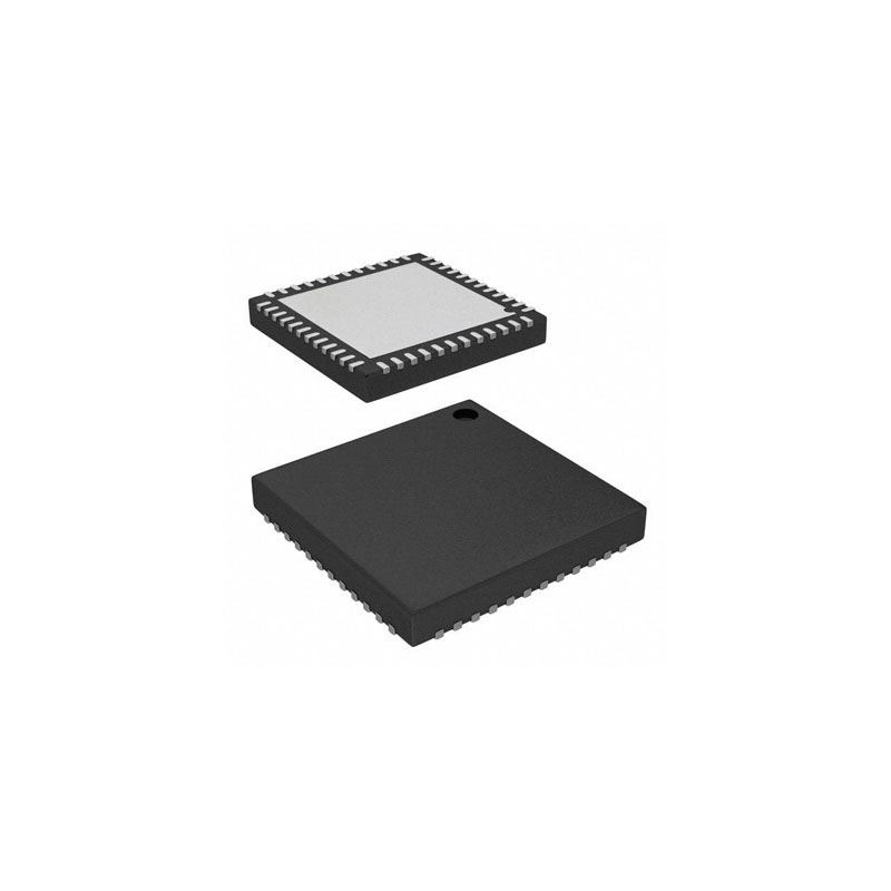
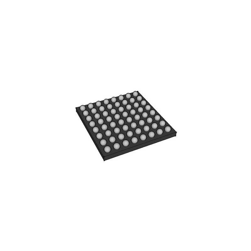
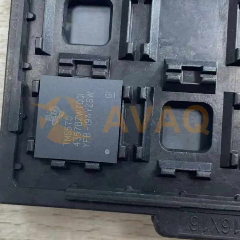
ARM® Cortex®-A8 Microprocessor IC OMAP-35xx 1 Core, 32-Bit 720MHz 515-POP-FCBGA (14x14)
Texas Instruments, Inc Inventory

Key Features

  • OMAP3530 and OMAP3525 Devices:
  • MPU Subsystem
  • NEON SIMD Coprocessor
  • High-Performance Image, Video, Audio (IVA2.2) Accelerator Subsystem
  • Up to 520-MHz TMS320C64x+ DSP Core
  • Enhanced Direct Memory Access (EDMA) Controller (128 Independent Channels)
  • Video Hardware Accelerators
  • Tile-Based Architecture Delivering up to 10 MPoly/sec
  • Universal Scalable Shader Engine: Multi-threaded Engine Incorporating Pixel and Vertex Shader Functionality
  • Industry Standard API Support: OpenGLES 1.1 and 2.0, OpenVG1.0
  • Fine-Grained Task Switching, Load Balancing, and Power Management
  • Programmable High-Quality Image Anti-Aliasing
  • Fully Software-Compatible with C64x and ARM9
  • Commercial and Extended Temperature Grades
  • Advanced Very-Long-Instruction-Word (VLIW) TMS320C64x+ DSP Core
  • Eight Highly Independent Functional Units
  • Six ALUs (32- and 40-Bit), Each Supports Single 32-Bit, Dual 16-Bit, or Quad 8-Bit Arithmetic per Clock Cycle
  • Two Multipliers Support Four 16 x 16-Bit Multiplies (32-Bit Results) per Clock Cycle or Eight 8 x 8-Bit Multiplies (16-Bit Results) per Clock Cycle
  • Load-Store Architecture with Nonaligned Support
  • 64 32-Bit General-Purpose Registers
  • Instruction Packing Reduces Code Size
  • All Instructions Conditional
  • Additional C64x+ Enhancements
  • Protected Mode Operation
  • Exceptions Support for Error Detection and Program Redirection
  • Hardware Support for Modulo Loop Operation
  • C64x+ L1 and L2 Memory Architecture
  • 32KB of L1P Program RAM and Cache (Direct Mapped)
  • 80KB of L1D Data RAM and Cache (2-Way Set-Associative)
  • 64KB of L2 Unified Mapped RAM and Cache (4-Way Set-Associative)
  • 32KB of L2 Shared SRAM and 16KB of L2 ROM
  • C64x+ Instruction Set Features
  • Byte-Addressable (8-, 16-, 32-, and 64-Bit Data)
  • 8-Bit Overflow Protection
  • Bit Field Extract, Set, Clear
  • Normalization, Saturation, Bit-Counting
  • Compact 16-Bit Instructions
  • Additional Instructions to Support Complex Multiplies
  • ARM Cortex-A8 Core
  • ARMv7 Architecture
  • TrustZone
  • Thumb-2
  • MMU Enhancements
  • In-Order, Dual-Issue, Superscalar Microprocessor Core
  • NEON Multimedia Architecture
  • Over 2x Performance of ARMv6 SIMD
  • Supports Both Integer and Floating-Point SIMD
  • Jazelle RCT Execution Environment Architecture
  • Dynamic Branch Prediction with Branch Target Address Cache, Global History Buffer, and 8-Entry Return Stack
  • Embedded Trace Macrocell (ETM) Support for Noninvasive Debug
  • ARM Cortex-A8 Memory Architecture:
  • 112KB of ROM
  • 64KB of Shared SRAM
  • Endianess:
  • ARM Instructions – Little Endian
  • ARM Data – Configurable
  • DSP Instruction and Data - Little Endian
  • External Memory Interfaces:
  • SDRAM Controller (SDRC)
  • 16- and 32-Bit Memory Controller with 1GB of Total Address Space
  • Interfaces to Low-Power Double Data Rate (LPDDR) SDRAM
  • SDRAM Memory Scheduler (SMS) and Rotation Engine
  • General Purpose Memory Controller (GPMC)
  • 16-Bit-Wide Multiplexed Address and Data Bus
  • Up to 8 Chip-Select Pins with 128-MB Address Space per Chip-Select Pin
  • Glueless Interface to NOR Flash, NAND Flash (with ECC Hamming Code Calculation), SRAM, and Pseudo-SRAM
  • Flexible Asynchronous Protocol Control for Interface to Custom Logic (FPGA, CPLD, ASICs, and so forth)
  • Nonmultiplexed Address and Data Mode (Limited 2-KB Address Space)
  • System Direct Memory Access (sDMA) Controller (32 Logical Channels with Configurable Priority)
  • Camera Image Signal Processor (ISP)
  • CCD and CMOS Imager Interface
  • Memory Data Input
  • BT.601 (8-Bit) and BT.656 (10-Bit) Digital YCbCr 4:2:2 Interface
  • Glueless Interface to Common Video Decoders
  • Resize Engine
  • Resize Images From 1/4x to 4x
  • Separate Horizontal and Vertical Control
  • Display Subsystem
  • Parallel Digital Output
  • Up to 24-Bit RGB
  • HD Maximum Resolution
  • Supports Up to 2 LCD Panels
  • Support for Remote Frame Buffer Interface (RFBI) LCD Panels
  • 2 10-Bit Digital-to-Analog Converters (DACs) Supporting:
  • Composite NTSC and PAL Video
  • Luma and Chroma Separate Video (S-Video)
  • Rotation 90-, 180-, and 270-Degrees
  • Resize Images From 1/4x to 8x
  • Color Space Converter
  • 8-Bit Alpha Blending
  • Serial Communication
  • 5 Multichannel Buffered Serial Ports (McBSPs)
  • 512-Byte Transmit and Receive Buffer (McBSP1, McBSP3, McBSP4, and McBSP5)
  • 5-KB Transmit and Receive Buffer (McBSP2)
  • SIDETONE Core Support (McBSP2 and McBSP3 Only) For Filter, Gain, and Mix Operations
  • Direct Interface to I2S and PCM Device and TDM Buses
  • 128-Channel Transmit and Receive Mode
  • Four Master or Slave Multichannel Serial Port Interface (McSPI) Ports
  • High-, Full-, and Low-Speed USB OTG Subsystem (12- and 8-Pin ULPI Interface)
  • High-, Full-, and Low-Speed Multiport USB Host Subsystem
  • 12- and 8-Pin ULPI Interface or 6-, 4-, and 3-Pin Serial Interface
  • Supports Transceiverless Link Logic (TLL)
  • One HDQ/1-Wire Interface
  • Three Master and Slave High-Speed Inter-Integrated Circuit (I2C) Controllers
  • Removable Media Interfaces:
  • Three Multimedia Card (MMC)/Secure Digital (SD) with Secure Data I/O (SDIO)
  • Comprehensive Power, Reset, and Clock Management
  • SmartReflex Technology
  • Dynamic Voltage and Frequency Scaling (DVFS)
  • Test Interfaces
  • IEEE 1149.1 (JTAG) Boundary-Scan Compatible
  • ETM Interface
  • Serial Data Transport Interface (SDTI)
  • 12 32-Bit General-Purpose Timers
  • 2 32-Bit Watchdog Timers
  • 1 32-Bit 32-kHz Sync Timer
  • Up to 188 General-Purpose I/O (GPIO) Pins (Multiplexed with Other Device Functions)
  • Package-On-Package (POP) Implementation for Memory Stacking (Not Available in CUS Package)
  • Discrete Memory Interface (Not Available in CBC Package)
  • Packages:
  • 515-pin s-PBGA Package (CBB Suffix),
  • 515-pin s-PBGA Package (CBC Suffix),
  • 423-pin s-PBGA Package (CUS Suffix),
  • 1.8-V I/O and 3.0-V (MMC1 Only),
Texas Instruments, Inc Original Stock
Texas Instruments, Inc Inventory

Specifications

Product Category: Processors - Application Specialized Shipping Restrictions: This product may require additional documentation to export from the United States.
Mounting Style: SMD/SMT Series: OMAP3530
Application: Audio Applications Core: ARM Cortex A8, TMS320C64x
Number of Cores: 2 Core Data Bus Width: 32 bit
Maximum Clock Frequency: 720 MHz, 520 MHz L1 Cache Instruction Memory: 16 kB, 32 kB
L1 Cache Data Memory: 16 kB, 80 kB Operating Supply Voltage: 985 mV to 1.35 V
Minimum Operating Temperature: 0 C Maximum Operating Temperature: + 90 C
Data RAM Size: 64 kB Data ROM Size: 112 kB, 16 kB
I/O Voltage: 1.8 V Interface Type: 1-Wire, I2C, Serial, UART, USB
L2 Cache Instruction / Data Memory: 256 kB, 96 kB Memory Type: L1/L2 Cache, ROM, SRAM
Moisture Sensitive: Yes Number of I/Os: 188 I/O
Number of Timers/Counters: 12 Timer Processor Series: OMAP
Product Type: Processors - Application Specialized Factory Pack Quantity: 119
Subcategory: Processors - Application Specialized Tradename: OMAP
Watchdog Timers: Watchdog Timer

Service Policies and Others

After-Sales & Settlement Related

payment Payment

Payment Method

hsbc
TT/Wire Transfer
paypal
Paypal
wu
Western Union
mg
Money Gram

For alternative payment channels, please reach out to us at:

[email protected]
shipping Shipping & Packing

Shipping Method

fedex
Fedex
ups
UPS
dhl
DHL
tnt
NTN
Packing

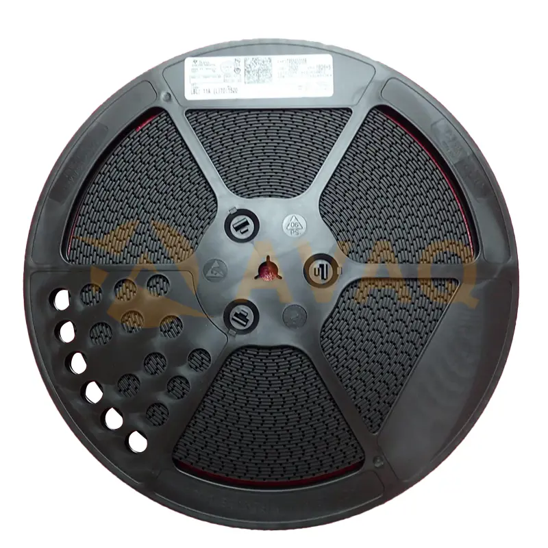
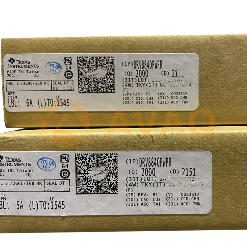
AVAQ determines and packages all devices based on electrostatic discharge (ESD) and moisture sensitivity level (MSL) protection requirements.

Warranty Warranty

We promise to provide 365 days quality assurance service for all our products.

Reviews

You need to log in to reply. Sign In | Sign Up

Availability: 6116 PCS

+BOM
Qty. Unit Price Ext. Price
1+ - -

The prices below are for reference only.