This website uses cookies. By using this site, you consent to the use of cookies. For more information, please take a look at our Privacy Policy.

O3853AQDCARQ1

Programmable Multi Channel PMIC 2.3V to 36V Automotive 48-Pin HTSSOP EP T/R

O3853AQDCARQ1 General Description

The TPS653853A-Q1 and TPS653854A-Q1 device is a multirail power supply designed to supply microcontrollers in safety relevant applications, such as those found in the automotive industry.

The device supports functional safety microcontrollers with dual-core lockstep (LS) and other multi-core architectures.

The TPS653853A-Q1 and TPS653854A-Q1 device integrates multiple supply rails to power the MCU, CAN or FlexRay, and external sensors. A buck-boost converter with internal FETs converts the input battery voltage between 2.3 V and 36 V to a 6-V preregulator output that supplies the other regulators. An integrated charge pump provides an overdrive voltage for the internal regulators, and can also be used to drive an external NMOS FET as reverse battery protection. The device supports wake-up from an ignition signal (IGN pin) or wake-up from a CAN transceiver or other signal (CAN_WU pin).

The device has a steering-angle monitoring (SAM) unit that allows the ECU to indirectly capture the position of the steering wheel through the motor-position sensors. A dedicated low-power mode allows this SAM unit to operate even when the ECU is in sleep mode. Integrated SAM-switches allow passing-through of the Motor-Position Sensor signals to the MCU during normal operation, or decoupling the MCU ADC inputs from the motor-position sensor signals when the ECU is in sleep mode.

An independent voltage monitoring unit inside the device monitors undervoltage and overvoltage on all internal supply rails and regulator outputs of the battery supply. Regulator current limits and temperature protections are also implemented. The TPS653853A-Q1 and TPS653854A-Q1 device features a question-answer watchdog, MCU error-signal monitor, clock monitoring on internal oscillator, self-check on clock monitor, cyclic redundancy check (CRC) on non-volatile memory and SPI communication, a diagnostic output pin allowing MCU to observe device internal analog and digital signals, a reset circuit for the MCU (NRES pin) and a safing output (ENDRV pin) to disable external power-stages on any detected system-failure. The device automatically runs a built-in self-test (BIST) at start up and the MCU may re-run the BIST during system run time through software control if needed. A dedicated DIAGNOSTIC state allows the MCU to check TPS653853A-Q1 and TPS653854A-Q1 functionality.

The TPS653853A-Q1 and TPS653854A-Q1 device also has an error reporting capability through the SPI register. The device has separate status bits in the SPI register for each specific error on the system level or device level. When the device detects a particular error condition, it sets the appropriate status bit and keeps this status bit set until the MCU reads-out the SPI register in which this status bit was set. Based on which status bit was set, the MCU can decide whether it must keep the system in a safe state or whether it can resume with the operation of the system.

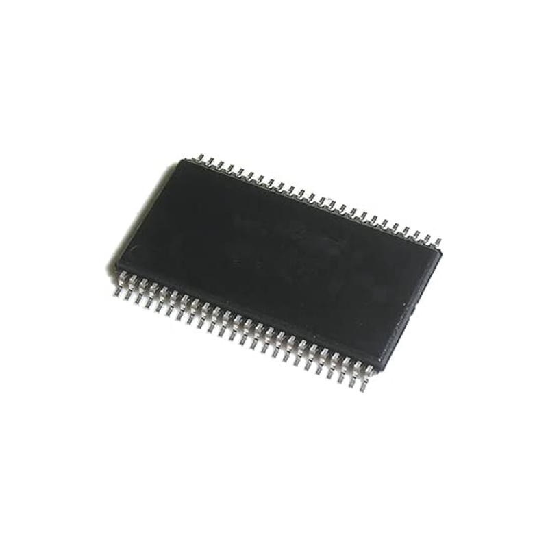
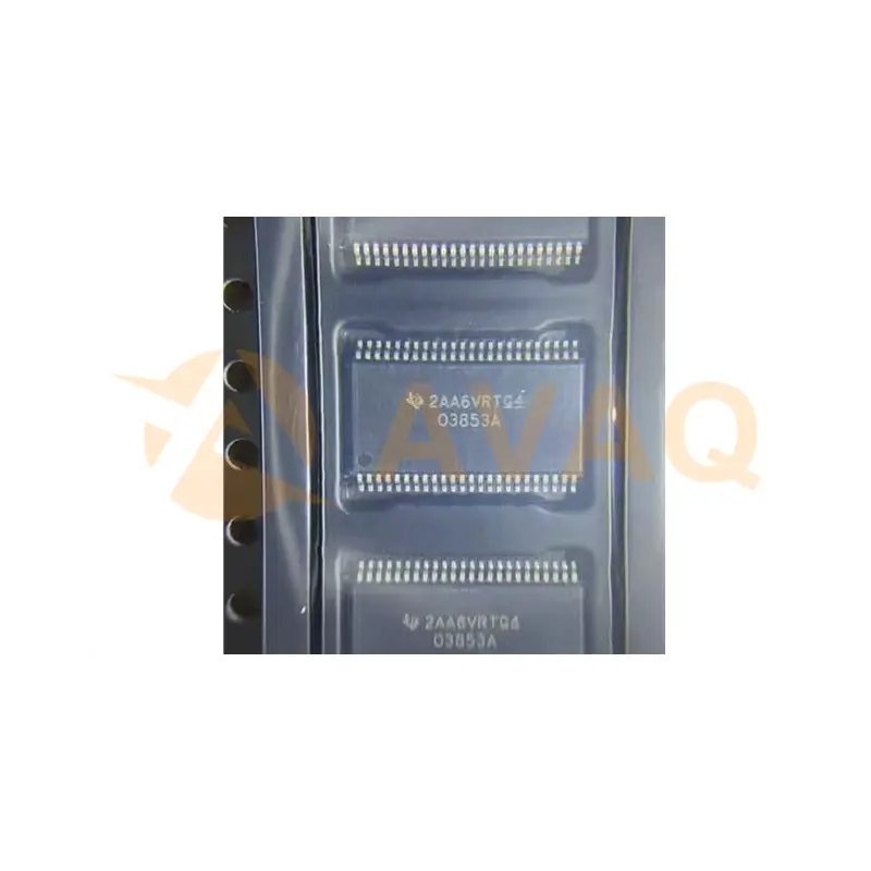
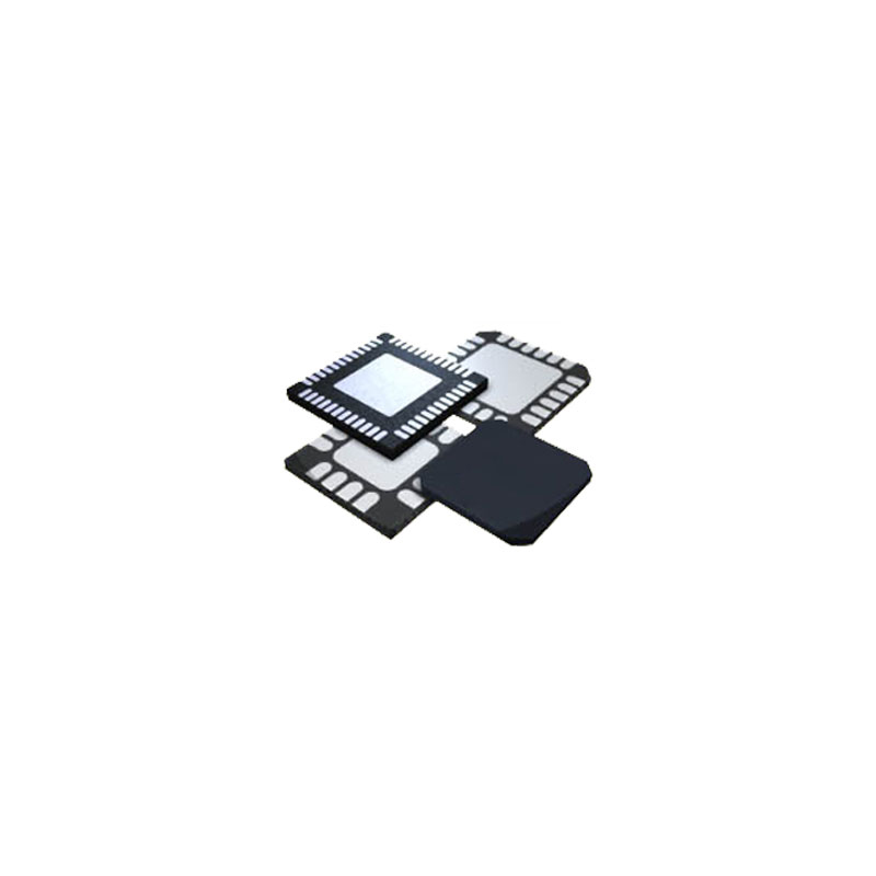
The TPS653853A-Q1 and TPS653854A-Q1 device is available in a 48-pin HTSSOP PowerPAD™ IC package.

O3853AQDCARQ1

Key Features

  • AEC-Q100 Qualified with the Following Results:
    • Device Temperature Grade 1: –40°C to +125°C Ambient Operating Temperature
    • Device HBM ESD Classification Level 2
    • Device CDM ESD Classification Level C4B
  • Functional Safety-Compliant
    • Developed for Functional Safety Applications
    • Documentation Available to Aid ISO 26262 System Design up to ASIL D
    • Systematic Capability and Hardware Integrity up to ASIL D
  • Input Voltage Range
    • 7 to 36-V for Initial Battery Power Up
    • 4 to 36-V Full Functionality After Initial Battery Power Up
    • Minimum 2.3 V During Operation After Wake-up
  • Supply Rails (With Internal FETs)
    • 6-V Synchronous Buck-Boost Preregulator
    • 5-V, 285-mA LDO (CAN, Peripherals or ADC REF 1% Accuracy with 20 to 120 mA Load)
    • 3.3-V or 5-V, 350-mA LDO (MCU) TPS653853A-Q1.3.3-V 350-mA or 5-V 500 mA LDO (MCU)TPS653854A-Q1
    • 2 LDOs Protected for Sensor Supply or Peripherals
      • 120 mA for Sensor Supply 1 (VSOUT1), 20 mA for Sensor Supply 2 (VSOUT2)
      • Configurable Tracking Mode (Tracking Input Pin), or 3.3-V or 5-V Fixed Output Voltage
      • Short-to-Ground and Battery Protection
    • Charge Pump: 6-V Minimum, 11-V Maximum Above Battery Voltage
  • Monitoring and Protection
    • Independent Undervoltage and Overvoltage Monitoring on All Regulator Outputs, Battery Voltage, and Internal Supplies
    • Voltage Monitoring Circuitry, Including Independent Bandgap Reference, Supplied from Separate Battery Voltage Input Pin
    • Self-Check on All Voltage Monitoring (During Power-Up and After Power-Up Initiated by External MCU)
    • All Supplies Protected with Current Limit and Overtemperature Prewarning and Shutdown
  • Steering-Angle Monitoring (SAM)
    • 2 Signal Comparators for Position Sensor Signals
    • Rotation Counter
    • Low-Power Mode With Periodically Sampling of Position Sensor Signals
    • Switches for Passing-Through Sensor Signals to MCU
  • Microcontroller Interface
    • Open and Close Window or Question-Answer Watchdog Function
    • Monitor for Functional Safety MCU Fault output (PWM or level), MCU Error-Signal Monitor
    • DIAGNOSTIC state for Performing Device Self-Tests and System Diagnostics
    • SAFE State for Device and System Protection upon Detected System Failure
    • Clock Monitor for Internal Oscillator
    • Analog and Logic Built-In Self-Test
    • CRC on Non-Volatile Memory as well as Device and System Configuration Registers and SPI Communications
    • Reset Circuit for MCU
    • Diagnostic Output Pin
  • SPI With CRC on Command Plus Data
  • Error Reporting Through SPI Registers for Errors on System Level and Device Level
  • Enable-Drive Output for Disabling External Power-Stages on Any Detected System Failure
  • Wake-up through IGN Pin (Ignition) or CAN_WU Pin (Transceiver or Other Function)
  • 48-Pin HTSSOP PowerPAD™ IC Package

Specifications

Regulated outputs (#) 5 TI functional safety category Functional Safety-Compliant
Vin (min) (V) 2.3 Vin (max) (V) 40
Iout (max) (A) 1 Configurability Software configurable
Rating Automotive Step-down DC/DC controller 0
Step-down DC/DC converter 0 Step-up DC/DC controller 0
Step-up DC/DC converter 0 LDO 4
Iq (typ) (mA) 0.032 Switching frequency (max) (kHz) 2100
Features Diagnostics, MCU interface, Power supply and system monitoring Operating temperature range (°C) -40 to 125
Processor name Aurix TC2x, Aurix TC3x, Aurix TC4x, C2000, Hercules TMS570, MPC56x, MPC57x, RH850, SPC56x, SPC57x, SPC58x Processor supplier Infineon, NXP/Freescale, Renesas, STMicroelectronics, Texas Instruments
Switching frequency (typ) (kHz) 2000

Service Policies and Others

After-Sales & Settlement Related

payment Payment

Payment Method

hsbc
TT/Wire Transfer
paypal
Paypal
wu
Western Union
mg
Money Gram

For alternative payment channels, please reach out to us at:

[email protected]
shipping Shipping & Packing

Shipping Method

fedex
Fedex
ups
UPS
dhl
DHL
tnt
NTN
Packing

AVAQ determines and packages all devices based on electrostatic discharge (ESD) and moisture sensitivity level (MSL) protection requirements.

Warranty Warranty

We promise to provide 365 days quality assurance service for all our products.

Ratings and Reviews

More
A
A**a 04/03/2020

All right. I'm happy with the purchase very much.

14

Reviews

You need to log in to reply. Sign In | Sign Up

Availability: 3258 PCS

+BOM
Qty. Unit Price Ext. Price
1+ - -

The prices below are for reference only.