Payment Method


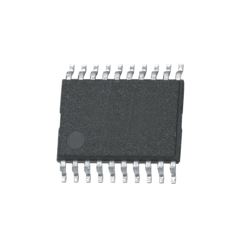
2-bit bidirectional multi-voltage level translator; open-drain; push-pull
TSSOPManufacturer:
Mfr.Part #:
LSF0102DP-Q100H
Datasheet:
Series:
Automotive, AEC-Q100
Translator Type:
Voltage Level
Channel Type:
Bidirectional
Number Of Circuits:
1
EDA/CAD Models:
Please fill in the short form below and we will provide you the quotation immediately.
The LSF0102-Q100 is a 2 channel bidirectional multi-voltage level translator for open-drain and push-pull applications. It supports up to 100 MHz up translation and ≥100 MHz down translation at ≤ 30 pF capacitive load. There is no need for a direction pin which minimizes system effort. The LSF0102-Q100 supports 5 V tolerant I/O pins for compatibility with TTL levels in a variety of applications. The ability to set up different voltage translation levels on each channel makes the device very flexible and suitable for a lot of different applications.This product has been qualified to the Automotive Electronics Council (AEC) standard Q100 (Grade 1) and is suitable for use in automotive applications.
| Category | Integrated Circuits (ICs)LogicTranslators, Level Shifters | Series | Automotive, AEC-Q100 |
| Translator Type | Voltage Level | Channel Type | Bidirectional |
| Number of Circuits | 1 | Channels per Circuit | 2 |
| Voltage - VCCA | 0 V ~ 5 V | Voltage - VCCB | 0 V ~ 5 V |
| Input Signal | - | Output Signal | - |
| Output Type | Open Drain, Push-Pull | Data Rate | - |
| Operating Temperature | -40°C ~ 125°C (TA) | Features | - |
| Mounting Type | Surface Mount | Base Product Number | LSF0102 |
After-Sales & Settlement Related
 Payment
Payment Method


For alternative payment channels, please reach out to us at:
[email protected] Shipping & Packing
Shipping Method


AVAQ determines and packages all devices based on electrostatic discharge (ESD) and moisture sensitivity level (MSL) protection requirements.
 Warranty

365-Day Product
Quality Guarantee
We promise to provide 365 days quality assurance service for all our products.
| Qty. | Unit Price | Ext. Price |
|---|---|---|
| 1+ | $0.469 | $0.47 |
| 10+ | $0.380 | $3.80 |
| 30+ | $0.342 | $10.26 |
| 100+ | $0.294 | $29.40 |
| 500+ | $0.274 | $137.00 |
| 1000+ | $0.261 | $261.00 |
The prices below are for reference only.
All bill of materials (BOM) can be sent via email to ![]() [email protected],
or fill below form to Quote for LSF0102DP-Q100H, guaranteed quotes back within
[email protected],
or fill below form to Quote for LSF0102DP-Q100H, guaranteed quotes back within
![]() 12hr.
12hr.
LSF0108PWJ
Nexperia
1000+ $0.202

HEF4094BT,653
Nexperia
5000+ $0.103

LSF0102GSX
Nexperia Semiconductor (NXP)
2-bit bidirectional multi-voltage level translator; open-drain; push-pull
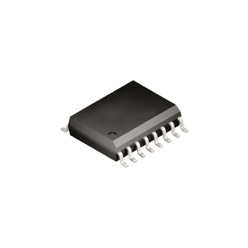
NPIC6C596ADJ
Nexperia Semiconductor (NXP)
Shift Shift Register 1 Element 8 Bit 16-SO
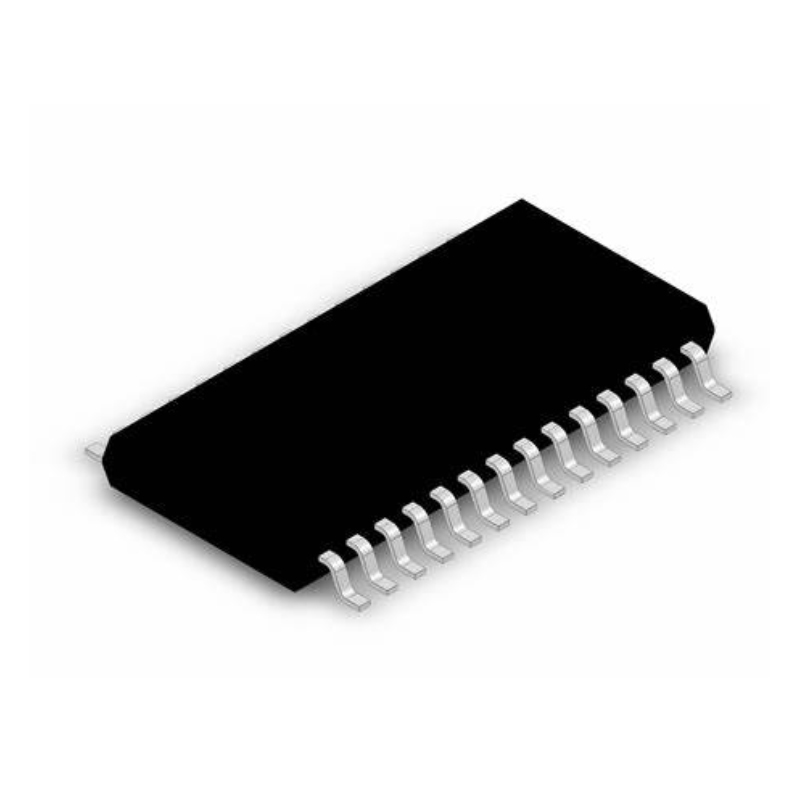
LSF0102DPH
Nexperia Semiconductor (NXP)
2-bit bidirectional multi-voltage level translator; open-drain; push-pull
