Payment Method


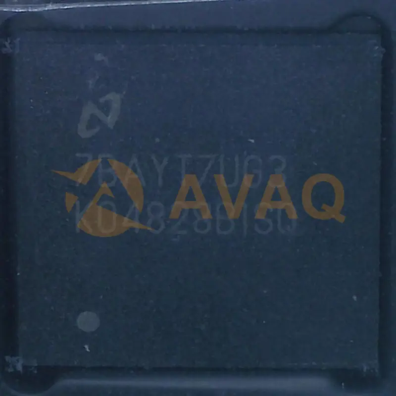
Jitter Cleaner IC 3.08GHz 1 64-WFQFN Exposed Pad
Manufacturer:
Mfr.Part #:
LMK04828BISQ/NOPB
Datasheet:
Pbfree Code:
Yes
Part Life Cycle Code:
Active
Reach Compliance Code:
compliant
ECCN Code:
EAR99
EDA/CAD Models:
Please fill in the short form below and we will provide you the quotation immediately.
The LMK0482x family is the industrys highest performance clock conditioner with JEDEC JESD204B support.
The 14 clock outputs from PLL2 can be configured to drive seven JESD204B converters or other logic devices, using device and SYSREF clocks. SYSREF can be provided using both DC and AC coupling. Not limited to JESD204B applications, each of the 14 outputs can be individually configured as high-performance outputs for traditional clocking systems.
The high performance, combined with features such as the ability to trade off between power or performance, dual VCOs, dynamic digital delay, holdover, and glitchless analog delay, make the LMK0482x family ideal for providing flexible high-performance clocking trees.
| Source Content uid | LMK04828BISQ/NOPB | Pbfree Code | Yes |
| Part Life Cycle Code | Active | Reach Compliance Code | compliant |
| ECCN Code | EAR99 | HTS Code | 8542.39.00.01 |
| JESD-30 Code | S-XQCC-N64 | Moisture Sensitivity Level | 3 |
| Number of Terminals | 64 | Peak Reflow Temperature (Cel) | 260 |
| Surface Mount | YES | Technology | CMOS |
| Temperature Grade | INDUSTRIAL | Terminal Finish | MATTE TIN |
| Terminal Form | NO LEAD | Terminal Position | QUAD |
| Time@Peak Reflow Temperature-Max (s) | 30 | uPs/uCs/Peripheral ICs Type | CLOCK GENERATOR, OTHER |
After-Sales & Settlement Related
 Payment
Payment Method


For alternative payment channels, please reach out to us at:
[email protected] Shipping & Packing
Shipping Method


AVAQ determines and packages all devices based on electrostatic discharge (ESD) and moisture sensitivity level (MSL) protection requirements.
 Warranty

365-Day Product
Quality Guarantee
We promise to provide 365 days quality assurance service for all our products.
| Qty. | Unit Price | Ext. Price |
|---|---|---|
| 1+ | - | - |
The prices below are for reference only.
All bill of materials (BOM) can be sent via email to ![]() [email protected],
or fill below form to Quote for LMK04828BISQ/NOPB, guaranteed quotes back within
[email protected],
or fill below form to Quote for LMK04828BISQ/NOPB, guaranteed quotes back within
![]() 12hr.
12hr.
