Payment Method


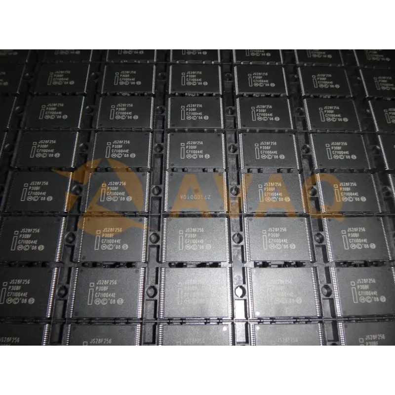
NOR Flash Parallel/Serial 1.8V 256M-bit 16M x 16 110ns 56-Pin TSOP Tray
Manufacturer:
Micron Technology
Mfr.Part #:
JS28F256P30BFE
Datasheet:
Pbfree Code:
Yes
Part Life Cycle Code:
Obsolete
Reach Compliance Code:
compliant
ECCN Code:
EAR99
EDA/CAD Models:
Please fill in the short form below and we will provide you the quotation immediately.
| Pbfree Code | Yes | Part Life Cycle Code | Obsolete |
| Reach Compliance Code | compliant | ECCN Code | EAR99 |
| HTS Code | 8542.32.00.51 | Access Time-Max | 20 ns |
| Additional Feature | IT ALSO HAVE ASYNCHRONOUS OPERATING MODE | Boot Block | BOTTOM |
| Command User Interface | YES | Common Flash Interface | YES |
| Data Polling | NO | JESD-30 Code | R-PDSO-G56 |
| JESD-609 Code | e3 | Length | 18.4 mm |
| Memory Density | 268435456 bit | Memory IC Type | FLASH |
| Memory Width | 16 | Number of Functions | 1 |
| Number of Sectors/Size | 4,255 | Number of Terminals | 56 |
| Number of Words | 16777216 words | Number of Words Code | 16000000 |
| Operating Mode | SYNCHRONOUS | Operating Temperature-Max | 85 °C |
| Operating Temperature-Min | -40 °C | Organization | 16MX16 |
| Parallel/Serial | PARALLEL | Programming Voltage | 1.8 V |
| Qualification Status | Not Qualified | Seated Height-Max | 1.025 mm |
| Sector Size | 16K,64K | Standby Current-Max | 0.00021 A |
| Supply Current-Max | 0.031 mA | Supply Voltage-Max (Vsup) | 2 V |
| Supply Voltage-Min (Vsup) | 1.7 V | Supply Voltage-Nom (Vsup) | 1.8 V |
| Surface Mount | YES | Technology | CMOS |
| Temperature Grade | INDUSTRIAL | Terminal Finish | MATTE TIN |
| Terminal Form | GULL WING | Terminal Pitch | 0.5 mm |
| Terminal Position | DUAL | Toggle Bit | NO |
| Type | NOR TYPE | Width | 14 mm |
After-Sales & Settlement Related
 Payment
Payment Method


For alternative payment channels, please reach out to us at:
[email protected] Shipping & Packing
Shipping Method


AVAQ determines and packages all devices based on electrostatic discharge (ESD) and moisture sensitivity level (MSL) protection requirements.
 Warranty

365-Day Product
Quality Guarantee
We promise to provide 365 days quality assurance service for all our products.
| Qty. | Unit Price | Ext. Price |
|---|---|---|
| 1+ | - | - |
The prices below are for reference only.
All bill of materials (BOM) can be sent via email to ![]() [email protected],
or fill below form to Quote for JS28F256P30BFE, guaranteed quotes back within
[email protected],
or fill below form to Quote for JS28F256P30BFE, guaranteed quotes back within
![]() 12hr.
12hr.
