Payment Method


Clock Buffer ISP Zero Delay Unv F an-Out Buf-Sngl End
Manufacturer:
Mfr.Part #:
ispPAC-CLK5312S-01T48C
Datasheet:
Series:
ispClock™
Programmable:
Not Verified
Type:
Clock Generator, Fanout Distribution, Zero Delay Buffer
PLL:
Yes with Bypass
EDA/CAD Models:
Please fill in the short form below and we will provide you the quotation immediately.
The ispClock5300S is an in-system-programmable zero delay universal fan-out buffer for use in clock distributionapplications. The ispClock5312S, the first member of the ispClock5300S family, provides up to 12 single-endedultra low skew outputs. Each pair of outputs may be independently configured to support separate I/O standards(LVTTL, LVCMOS -3.3V, 2.5V, 1.8, SSTL, HSTL) and output frequency. In addition, each output provides independent programmable control of termination, slew-rate, and timing skew. All configuration information is stored onchip in non-volatile E2CMOS® memory.
The ispClock5300S devices provide extremely low propagation delay (zero-delay) from input to output using theon-chip low jitter high-performance PLL. A set of three programmable 5-bit counters can be used to generate threefrequencies derived from the PLL clock. These counters are programmable in powers of 2 only (1, 2, 4, 8, 16, 32).The clock output from any of the V-dividers can then be routed to any clock output pin through the output routingmatrix. The output routing matrix, in addition, also enables routing of reference clock inputs directly to any output.The ispClock5300S device can be configured to operate in four modes: zero delay buffer mode, dual non-zerodelay buffer mode, non-zero delay buffer mode with output dividers, and combined zero-delay and non-zero delaybuffer mode.
| Category | Integrated Circuits (ICs)Clock/TimingClock Generators, PLLs, Frequency Synthesizers | Series | ispClock™ |
| Programmable | Not Verified | Type | Clock Generator, Fanout Distribution, Zero Delay Buffer |
| PLL | Yes with Bypass | Input | HSTL, LVCMOS, LVDS, LVPECL, LVTTL, SSTL |
| Output | eHSTL, HSTL, LVCMOS, LVTTL, SSTL | Number of Circuits | 1 |
| Ratio - Input:Output | 2:12 | Differential - Input:Output | Yes/No |
| Frequency - Max | 267MHz | Divider/Multiplier | Yes/No |
| Voltage - Supply | 3V ~ 3.6V | Operating Temperature | 0°C ~ 70°C |
| Mounting Type | Surface Mount | Base Product Number | ISPPAC-CLK53 |
| Product Category | Clock Buffer | Number of Outputs | 12 Output |
| Maximum Input Frequency | 400 MHz | Supply Voltage - Max | 3.6 V |
| Supply Voltage - Min | 3 V | Propagation Delay - Max | 6.5 ns |
| Minimum Operating Temperature | 0 C | Maximum Operating Temperature | + 70 C |
| Mounting Style | SMD/SMT | Duty Cycle - Max | 53 % |
| Max Output Freq | 267 MHz | Moisture Sensitive | Yes |
| Operating Supply Current | 7 mA | Product | Clock Buffers |
| Product Type | Clock Buffers | Factory Pack Quantity | 250 |
| Subcategory | Clock & Timer ICs | Tradename | ispClock |
| Unit Weight | 0.319998 oz |
After-Sales & Settlement Related
 Payment
Payment Method


For alternative payment channels, please reach out to us at:
[email protected] Shipping & Packing
Shipping Method


AVAQ determines and packages all devices based on electrostatic discharge (ESD) and moisture sensitivity level (MSL) protection requirements.
 Warranty

365-Day Product
Quality Guarantee
We promise to provide 365 days quality assurance service for all our products.
| Qty. | Unit Price | Ext. Price |
|---|---|---|
| 1+ | - | - |
The prices below are for reference only.
All bill of materials (BOM) can be sent via email to ![]() [email protected],
or fill below form to Quote for ispPAC-CLK5312S-01T48C, guaranteed quotes back within
[email protected],
or fill below form to Quote for ispPAC-CLK5312S-01T48C, guaranteed quotes back within
![]() 12hr.
12hr.
ISPPAC-CLK5510V-01T48I
LATTICE
IC 320MHz 1 48-LQFP

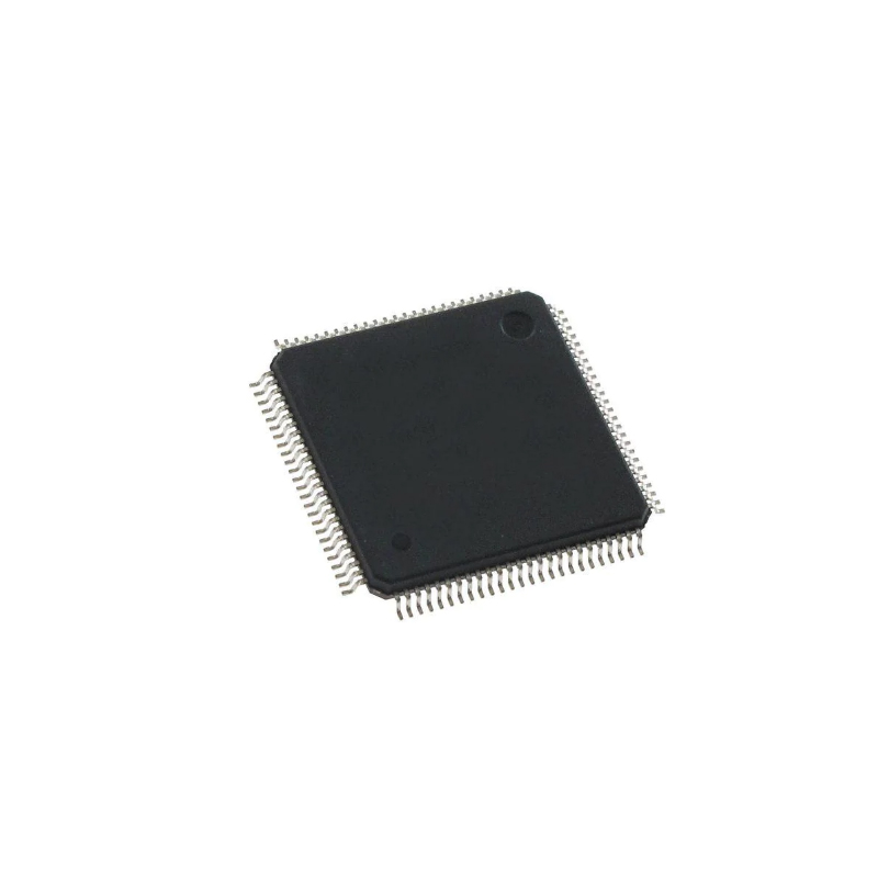
ISPPAC-CLK5520V-01T100I
Lattice
Clock Drivers & Distribution PROGRAMMABLE CLOCK GENERATOR
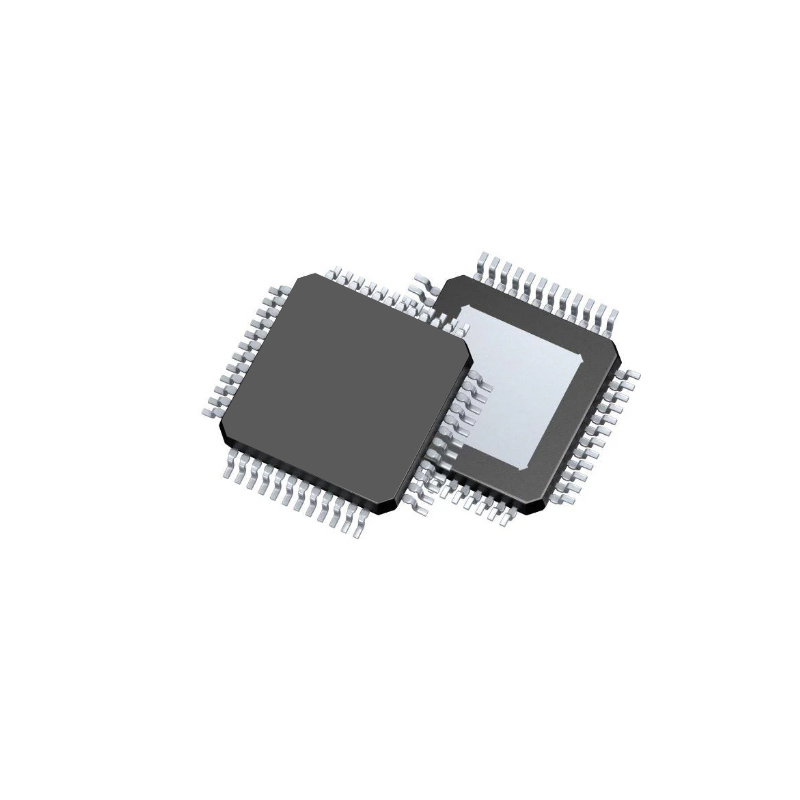
ISPPAC-CLK5312S-01T48I
Lattice
Clock Buffer ISP 0 Delay Unv Fan- Out Buf-Sngl End I

ISPPAC-CLK5308S-01T48I
Lattice
Zero Delay Buffer 8-Out eHSTL/HSTL/LVCMOS/LVTTL/SSTL Single-Ended 48-Pin TQFP Tray

ISPPAC-CLK5510V-01T48C
Lattice
Clock Drivers & Distribution PROGRAMMABLE CLOCK GENERATOR