Payment Method


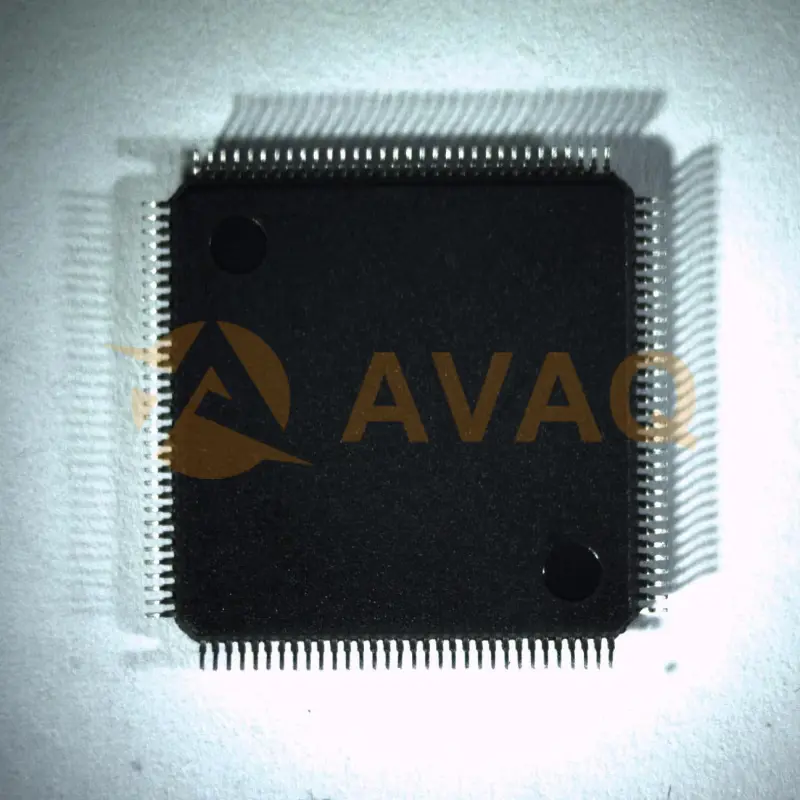
Low Speed/Full Speed/High Speed Host Controller USB 2.0/USB1.1 3.3V 128-Pin LQFP
Manufacturer:
Mfr.Part #:
ISP1563BMUM
Datasheet:
ECCN (US):
EAR99
HTS:
8541.29.00.95
Automotive:
No
PPAP:
No
Please fill in the short form below and we will provide you the quotation immediately.
Avaq Semiconductor offers the highly versatile and reliable ISP1563BMUM driver, produced by ST. With its multifunctional and high-performance capabilities, this component is an excellent choice for a wide range of electronic projects.
To ensure that you have all the necessary information to make the most of this component, Avaq provides a free datasheet PDF, as well as circuit diagrams, pin layouts, pin details, pin voltage ratings, and equivalent components for the ISP1563BMUM.
Avaq also offers free samples. Simply fill out and submit the sample request form to receive your free samples for testing. If you have any questions, please feel free to contact us at any time.
| ECCN (US) | EAR99 | Part Status | Active |
| HTS | 8541.29.00.95 | Automotive | No |
| PPAP | No | Category | Power MOSFET |
| Configuration | Single | Channel Mode | Enhancement |
| Channel Type | P | Number of Elements per Chip | 1 |
| Maximum Drain Source Voltage (V) | 100 | Maximum Gate Source Voltage (V) | ±20 |
| Maximum Gate Threshold Voltage (V) | 3 | Operating Junction Temperature (°C) | -55 to 150 |
| Maximum Continuous Drain Current (A) | 9 | Maximum Gate Source Leakage Current (nA) | 100 |
| Maximum IDSS (uA) | 1 | Maximum Drain Source Resistance (mOhm) | 240@10V |
| Typical Gate Charge @ Vgs (nC) | 17.5@10V|[email protected] | Typical Gate Charge @ 10V (nC) | 17.5 |
| Typical Gate to Drain Charge (nC) | 3.2 | Typical Gate to Source Charge (nC) | 2.8 |
| Typical Reverse Recovery Charge (nC) | 24.5 | Typical Input Capacitance @ Vds (pF) | 1239@25V |
| Typical Reverse Transfer Capacitance @ Vds (pF) | 28@25V | Minimum Gate Threshold Voltage (V) | 1 |
| Typical Output Capacitance (pF) | 42 | Maximum Power Dissipation (mW) | 42000 |
| Typical Fall Time (ns) | 34.4 | Typical Rise Time (ns) | 14.9 |
| Typical Turn-Off Delay Time (ns) | 57.4 | Typical Turn-On Delay Time (ns) | 9.1 |
| Minimum Operating Temperature (°C) | -55 | Maximum Operating Temperature (°C) | 150 |
| Supplier Temperature Grade | Automotive | Packaging | Tape and Reel |
| Maximum Power Dissipation on PCB @ TC=25°C (W) | 42 | Maximum Pulsed Drain Current @ TC=25°C (A) | 15 |
| Maximum Junction Ambient Thermal Resistance on PCB (°C/W) | 44 | Typical Diode Forward Voltage (V) | 0.7 |
| Typical Gate Plateau Voltage (V) | 3.1 | Typical Reverse Recovery Time (ns) | 25.2 |
| Maximum Diode Forward Voltage (V) | 1.2 | Maximum Positive Gate Source Voltage (V) | 20 |
| Maximum Continuous Drain Current on PCB @ TC=25°C (A) | 9 | Mounting | Surface Mount |
| PCB changed | 2 | Tab | Tab |
| Pin Count | 3 | Lead Shape | Gull-wing |
After-Sales & Settlement Related
 Payment
Payment Method


For alternative payment channels, please reach out to us at:
[email protected] Shipping & Packing
Shipping Method


AVAQ determines and packages all devices based on electrostatic discharge (ESD) and moisture sensitivity level (MSL) protection requirements.
 Warranty

365-Day Product
Quality Guarantee
We promise to provide 365 days quality assurance service for all our products.
| Qty. | Unit Price | Ext. Price |
|---|---|---|
| 1+ | - | - |
The prices below are for reference only.
All bill of materials (BOM) can be sent via email to ![]() [email protected],
or fill below form to Quote for ISP1563BMUM, guaranteed quotes back within
[email protected],
or fill below form to Quote for ISP1563BMUM, guaranteed quotes back within
![]() 12hr.
12hr.
