This website uses cookies. By using this site, you consent to the use of cookies. For more information, please take a look at our Privacy Policy.

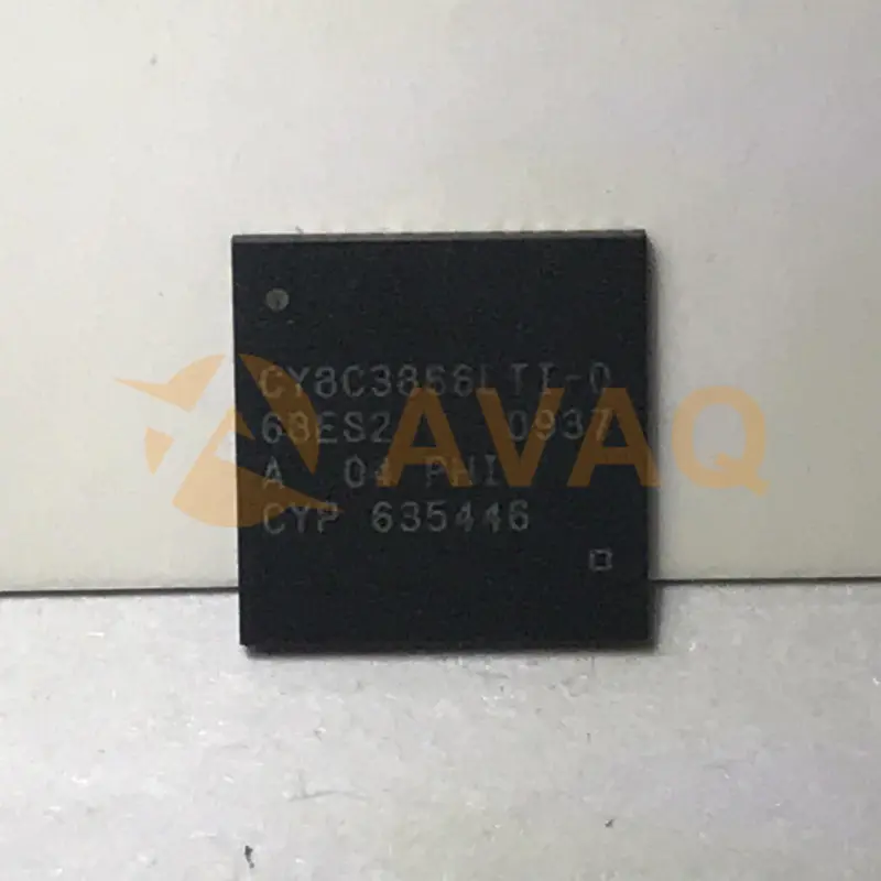
CY8C3866LTI-068

8-bit Microcontrollers - MCU 64K Flash 67MHz 8051 0.5V to 5.5V

CY8C3866LTI-068 General Description

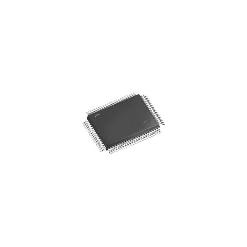
8051 PSOC® 3 CY8C38xx Microcontroller IC 8-Bit 67MHz 64KB (64K x 8) FLASH 48-QFN (7x7)

Key Features

  • Single cycle 8051 CPU
  • DC to 67 MHz operation
  • Multiply and divide instructions
  • Flash program memory, up to 64 KB, 100,000 write cycles, 20 years retention, and multiple security features
  • Up to 8-KB flash error correcting code (ECC) or configuration storage
  • Up to 8 KB SRAM
  • Up to 2 KB electrically erasable programmable read-only memory (EEPROM), 1 M cycles, and 20 years retention
  • 24-channel direct memory access (DMA) with multilayer AHB[1] bus access
  • Programmable chained descriptors and priorities
  • High bandwidth 32-bit transfer support
  • Low voltage, ultra low-power
  • Wide operating voltage range: 0.5 V to 5.5 V
  • High efficiency boost regulator from 0.5-V input through 1.8-V to 5.0-V output
  • 0.8 mA at 3 MHz, 1.2 mA at 6 MHz, and 6.6 mA at 48 MHz
  • Low-power modes including:
  • 1-µA sleep mode with real time clock and low-voltage detect (LVD) interrupt
  • 200-nA hibernate mode with RAM retention
  • Versatile I/O system
  • 28 to 72 I/O (62 GPIOs, eight special input/outputs (SIO), two USBIOs[2])
  • Any GPIO to any digital or analog peripheral routability
  • LCD direct drive from any GPIO, up to 46 × 16 segments[2]
  • CapSense® support from any GPIO[3]
  • 1.2-V to 5.5-V I/O interface voltages, up to four domains
  • Maskable, independent IRQ on any pin or port
  • Schmitt-trigger transistor-transistor logic (TTL) inputs
  • All GPIO configurable as open drain high/low, pull-up/pull-down, High Z, or strong output
  • Configurable GPIO pin state at power-on reset (POR)
  • 25 mA sink on SIO
  • Digital peripherals
  • 20 to 24 programmable logic device (PLD) based universal digital blocks (UDB)
  • Full CAN 2.0b 16 Rx, 8 Tx buffers[2]
  • Full-speed (FS) USB 2.0 12 Mbps using internal oscillator[2]
  • Up to four 16-bit configurable timer, counter, and PWM blocks
  • 67 MHz, 24-bit fixed point digital filter block (DFB) to implement FIR and IIR filters
  • Library of standard peripherals
  • 8-, 16-, 24-, and 32-bit timers, counters, and PWMs
  • Serial peripheral interface (SPI), universal asynchronous transmitter receiver (UART), and I2C
  • Many others available in catalog
  • Library of advanced peripherals
  • Cyclic redundancy check (CRC)
  • Pseudo random sequence (PRS) generator
  • Local interconnect network (LIN) bus 2.0
  • Quadrature decoder
  • Analog peripherals (1.71 V ≤ VDDA ≤ 5.5 V)
  • 1.024 V ± 0.1% internal voltage reference across –40 °C to +85 °C (14 ppm/°C)
  • Configurable delta-sigma ADC with 8- to 20-bit resolution
  • Sample rates up to 192 ksps
  • Programmable gain stage: ×0.25 to ×16
  • 12-bit mode, 192 ksps, 66-dB signal to noise and distortion ratio (SINAD), ±1-bit INL/DNL
  • 16-bit mode, 48 ksps, 84-dB SINAD, ±2-bit INL, ±1-bit DNL
  • Up to four 8-bit, 8-Msps IDACs or 1-Msps VDACs
  • Four comparators with 95-ns response time
  • Up to four uncommitted opamps with 25-mA drive capability
  • Up to four configurable multifunction analog blocks. Example configurations are programmable gain amplifier (PGA), transimpedance amplifier (TIA), mixer, and sample and hold
  • CapSense support
  • Programming, debug, and trace
  • JTAG (4-wire), serial wire debug (SWD) (2-wire), and single wire viewer (SWV) interfaces
  • Eight address and one data breakpoint
  • 4-KB instruction trace buffer
  • Bootloader programming supportable through I2C, SPI, UART, USB, and other interfaces
  • Precision, programmable clocking
  • 3- to 62-MHz internal oscillator over full temperature and voltage range
  • 4- to 25-MHz crystal oscillator for crystal PPM accuracy
  • Internal PLL clock generation up to 67 MHz
  • 32.768-kHz watch crystal oscillator
  • Low-power internal oscillator at 1, 33, and 100 kHz
  • Temperature and packaging
  • –40°C to +85 °C degrees industrial temperature
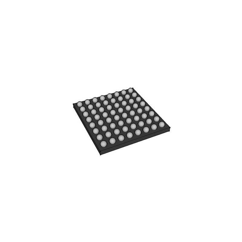
  • 48-pin SSOP, 48-pin QFN, 68-pin QFN, and 100-pin TQFP package options

Specifications

Part Life Cycle Code Active Reach Compliance Code compliant
Address Bus Width Boundary Scan YES
Clock Frequency-Max 67 MHz External Data Bus Width
JESD-30 Code S-XQCC-N48 JESD-609 Code e4
Length 7 mm Moisture Sensitivity Level 3
Number of I/O Lines 31 Number of Terminals 48
Operating Temperature-Max 85 °C Operating Temperature-Min -40 °C
Peak Reflow Temperature (Cel) 260 Qualification Status Not Qualified
RAM (words) 4096 Seated Height-Max 1 mm
Supply Voltage-Max 5.5 V Supply Voltage-Min 1.71 V
Supply Voltage-Nom 3.3 V Surface Mount YES
Technology CMOS Temperature Grade INDUSTRIAL
Terminal Finish NICKEL PALLADIUM GOLD Terminal Form NO LEAD
Terminal Pitch 0.5 mm Terminal Position QUAD
Time@Peak Reflow Temperature-Max (s) 20 Width 7 mm

Service Policies and Others

After-Sales & Settlement Related

payment Payment

Payment Method

hsbc
TT/Wire Transfer
paypal
Paypal
wu
Western Union
mg
Money Gram

For alternative payment channels, please reach out to us at:

[email protected]
shipping Shipping & Packing

Shipping Method

fedex
Fedex
ups
UPS
dhl
DHL
tnt
NTN
Packing

AVAQ determines and packages all devices based on electrostatic discharge (ESD) and moisture sensitivity level (MSL) protection requirements.

Warranty Warranty

We promise to provide 365 days quality assurance service for all our products.

Reviews

You need to log in to reply. Sign In | Sign Up

Availability: 6421 PCS

+BOM
Qty. Unit Price Ext. Price
1+ - -

The prices below are for reference only.