Payment Method


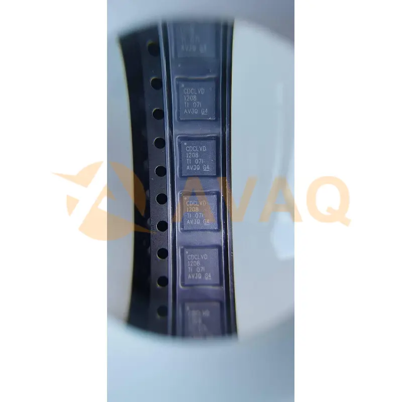
Low jitter, 2-input selectable 1:8 universal-to-LVDS buffer
Manufacturer:
Mfr.Part #:
CDCLVD1208RHDR
Datasheet:
Pbfree Code:
Yes
Part Life Cycle Code:
Active
Pin Count:
28
Reach Compliance Code:
compliant
EDA/CAD Models:
Please fill in the short form below and we will provide you the quotation immediately.
The CDCLVD1208 clock buffer distributes one of two selectable clock inputs (IN0 and IN1) to 8 pairs of differential LVDS clock outputs (OUT0 through OUT7) with minimum skew for clock distribution. The CDCLVD1208 can accept two clock sources into an input multiplexer. The inputs can either be LVDS, LVPECL, or LVCMOS.
The CDCLVD1208 is specifically designed for driving 50-Ω transmission lines. In case of driving the inputs in single-ended mode, the appropriate bias voltage, VAC_REF, must be applied to the unused negative input pin.
The IN_SEL pin selects the input which is routed to the outputs. If this pin is left open, it disables the outputs (static). The part supports a fail-safe function. The device incorporates an input hysteresis which prevents random oscillation of the outputs in the absence of an input signal.
The device operates in 2.5-V supply environment and is characterized from –40°C to 85°C (ambient temperature). The CDCLVD1208 is packaged in small, 28-pin, 5-mm × 5-mm VQFN package.
All other trademarks are the property of their respective owners
| Source Content uid | CDCLVD1208RHDR | Pbfree Code | Yes |
| Part Life Cycle Code | Active | Pin Count | 28 |
| Reach Compliance Code | compliant | ECCN Code | EAR99 |
| HTS Code | 8542.39.00.01 | Family | CDC |
| Input Conditioning | DIFFERENTIAL MUX | JESD-30 Code | S-PQCC-N28 |
| Logic IC Type | LOW SKEW CLOCK DRIVER | Moisture Sensitivity Level | 2 |
| Number of Functions | 1 | Number of Inverted Outputs | |
| Number of Terminals | 28 | Number of True Outputs | 8 |
| Packing Method | TR | Peak Reflow Temperature (Cel) | 260 |
| Surface Mount | YES | Temperature Grade | INDUSTRIAL |
| Terminal Finish | Nickel/Palladium/Gold (Ni/Pd/Au) | Terminal Form | NO LEAD |
| Terminal Position | QUAD | Time@Peak Reflow Temperature-Max (s) | NOT SPECIFIED |
After-Sales & Settlement Related
 Payment
Payment Method


For alternative payment channels, please reach out to us at:
[email protected] Shipping & Packing
Shipping Method


AVAQ determines and packages all devices based on electrostatic discharge (ESD) and moisture sensitivity level (MSL) protection requirements.
 Warranty

365-Day Product
Quality Guarantee
We promise to provide 365 days quality assurance service for all our products.
| Qty. | Unit Price | Ext. Price |
|---|---|---|
| 1+ | $5.554 | $5.55 |
| 10+ | $4.959 | $49.59 |
| 30+ | $4.577 | $137.31 |
| 100+ | $4.209 | $420.90 |
The prices below are for reference only.
All bill of materials (BOM) can be sent via email to ![]() [email protected],
or fill below form to Quote for CDCLVD1208RHDR, guaranteed quotes back within
[email protected],
or fill below form to Quote for CDCLVD1208RHDR, guaranteed quotes back within
![]() 12hr.
12hr.
