This website uses cookies. By using this site, you consent to the use of cookies. For more information, please take a look at our Privacy Policy.

CDCLVC1310RHBR

Universal input, 10-output low impedance LVCMOS buffer

CDCLVC1310RHBR General Description

The CDCLVC1310 is a highly versatile, low-jitter, low-power clock fanout buffer which can distribute to ten low-jitter LVCMOS clock outputs from one of three inputs, whose primary and secondary inputs can feature differential or single-ended signals and crystal input. Such a buffer is good for use in a variety of mobile and wired infrastructure, data communication, computing, low-power medical imaging, and portable test and measurement applications. When the input is an illegal level, the output is at a defined state. One can set the core to 2.5 V or 3.3 V, and output to 1.5 V, 1.8 V, 2.5 V or 3.3 V. Pin programming easily configures the CDCLVC1310. The overall additive jitter performance is 25 fsRMS (typical). The CDCLVC1310 comes in a small 32-pin 5-mm × 5-mm QFN package.

Texas Instruments, Inc Inventory

Key Features

  • High-Performance Crystal Buffer With Ultralow Noise
    Floor of –169 dBc/Hz
  • Additive Phase Noise/Jitter Performance Is
    25 fsRMS (Typ.)
  • Level Translation With 3.3-V or 2.5-V Core and
    3.3-V, 2.5-V, 1.8-V, or 1.5-V Output Supply
  • Device inputs consist of primary, secondary,
    and crystal inputs, and manually selectable
    (through pins) using the input MUX. The primary
    and secondary inputs can accept LVPECL, LVDS,
    HCSL, SSTL or LVCMOS signals and crystal input.
    • Crystal Frequencies Supported Are From
      8 MHz to 50 MHz
    • Differential and Single-Ended Input Frequencies
      Supported Are up to 200 MHz
  • 10 Single-Ended LVCMOS Outputs. The outputs can
    operate at 1.5-V, 1.8-V, 2.5-V or 3.3-V
    Power-Supply Voltage.
    • LVCMOS Outputs Operate up to 200 MHz
    • Output Skew Is 30 ps (Typical)
    • Total Propagation Delay Is 2 ns (Typical)
    • Synchronous and Glitch-Free Output Enable Is
      Available
  • Offered in QFN-32 5-mm × 5-mm Package With
    Industrial Temperature Range of –40°C to 85°C
  • Can Overdrive Crystal Input With LVCMOS Signal up to 50 MHz
Texas Instruments, Inc Original Stock
Texas Instruments, Inc Inventory

Specifications

Category Integrated Circuits (ICs)Clock/TimingClock Buffers, Drivers Series -
Type Fanout Buffer (Distribution), Multiplexer Number of Circuits 1
Ratio - Input:Output 3:10 Differential - Input:Output Yes/No
Input HCSL, LVCMOS, LVDS, LVPECL, SSTL, Crystal Output LVCMOS
Frequency - Max 200 MHz Voltage - Supply 2.375V ~ 3.465V
Operating Temperature -40°C ~ 85°C Mounting Type Surface Mount
Base Product Number CDCLVC1310

Service Policies and Others

After-Sales & Settlement Related

payment Payment

Payment Method

hsbc
TT/Wire Transfer
paypal
Paypal
wu
Western Union
mg
Money Gram

For alternative payment channels, please reach out to us at:

[email protected]
shipping Shipping & Packing

Shipping Method

fedex
Fedex
ups
UPS
dhl
DHL
tnt
NTN
Packing

AVAQ determines and packages all devices based on electrostatic discharge (ESD) and moisture sensitivity level (MSL) protection requirements.

Warranty Warranty

We promise to provide 365 days quality assurance service for all our products.

Ratings and Reviews

More
M
M**n 09/01/2022

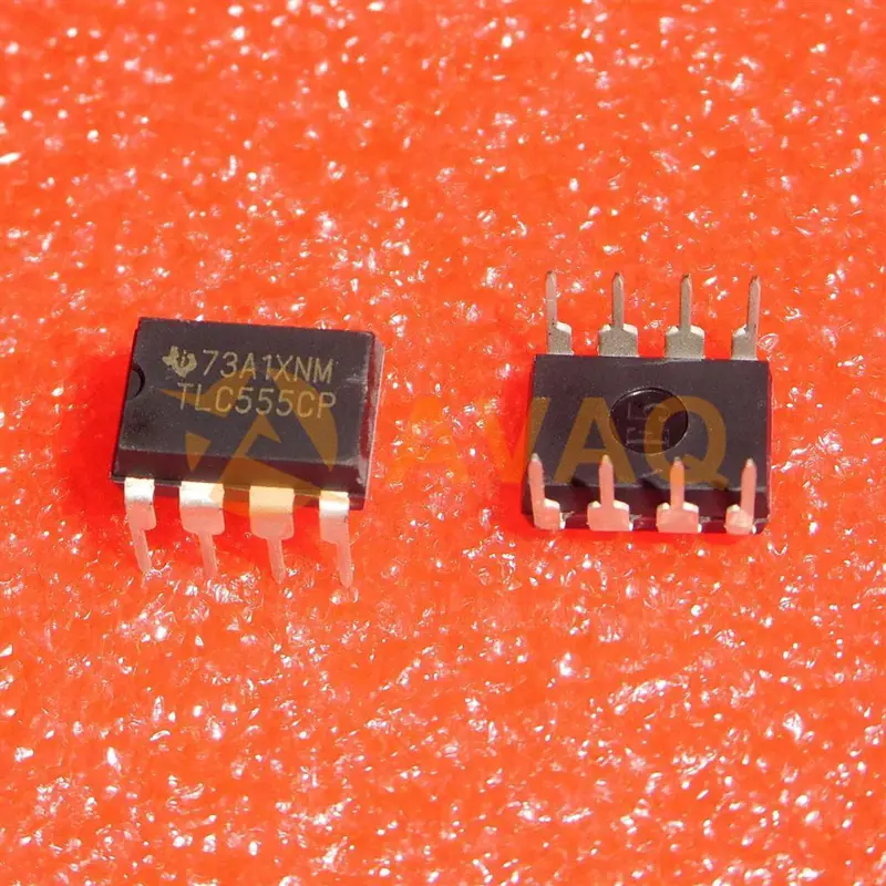
Honestly, it's easier to solder than to hook up with these crocodiles, xs why ordered to see somewhere in the reviews of repairers

14
O
O**n 08/02/2022

Everything is fine, a loud speaker for its size.

12
E
E**a 03/15/2022

perfect transaction Thank you

17
G
G**s 12/28/2020

Every deal is smooth, good supplier. Thank you for the business

3

Reviews

You need to log in to reply. Sign In | Sign Up

Availability: 5897 PCS

+BOM
Qty. Unit Price Ext. Price
1+ $2.913 $2.91
10+ $2.561 $25.61
30+ $2.350 $70.50
100+ $2.006 $200.60
500+ $1.908 $954.00
1000+ $1.863 $1,863.00

The prices below are for reference only.