This website uses cookies. By using this site, you consent to the use of cookies. For more information, please take a look at our Privacy Policy.

A3PE600-1PQG208I +BOM

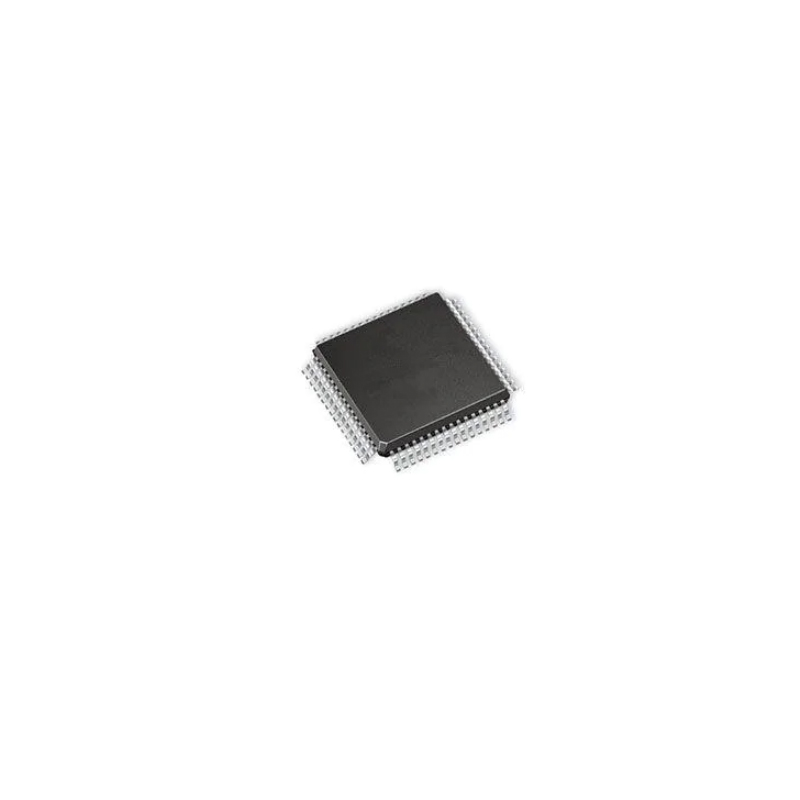
ProASIC3E Field Programmable Gate Array (FPGA) IC 147 110592 208-BFQFP

A3PE600-1PQG208I General Description

ProASIC3E Field Programmable Gate Array (FPGA) IC 147 110592 208-BFQFP

Key Features

  • High Capacity
  • 600 k to 3 Million System Gates
  • 108 to 504 kbits of True Dual-Port SRAM
  • Up to 620 User I/Os
  • Reprogrammable Flash Technology
  • 130-nm, 7-Layer Metal (6 Copper), Flash-Based CMOS Process
  • Instant On Level 0 Support
  • Single-Chip Solution
  • Retains Programmed Design when Powered Off
  • On-Chip User Nonvolatile Memory
  • 1 kbit of FlashROM with Synchronous Interfacing
  • High Performance
  • 350 MHz System Performance
  • 3.3 V, 66 MHz 64-Bit PCI
  • In-System Programming (ISP) and Security
  • ISP Using On-Chip 128-Bit Advanced Encryption Standard (AES) Decryption via JTAG (IEEE 1532–compliant)
  • FlashLock® Designed to Secure FPGA Contents
  • Low Power
  • Core Voltage for Low Power
  • Support for 1.5-V-Only Systems
  • Low-Impedance Flash Switches
  • High-Performance Routing Hierarchy
  • Segmented, Hierarchical Routing and Clock Structure
  • Ultra-Fast Local and Long-Line Network
  • Enhanced High-Speed, Very-Long-Line Network
  • High-Performance, Low-Skew Global Network
  • Architecture Supports Ultra-High Utilization
  • Pro (Professional) I/O
  • 700 Mbps DDR, LVDS-Capable I/Os
  • 1.5 V, 1.8 V, 2.5 V, and 3.3 V Mixed-Voltage Operation
  • Bank-Selectable I/O Voltages—up to 8 Banks per Chip
  • Single-Ended I/O Standards: LVTTL, LVCMOS 3.3 V / 2.5 V / 1.8 V / 1.5 V, 3.3 V PCI / 3.3 V PCI-X, and LVCMOS 2.5 V / 5.0 V Input
  • Differential I/O Standards: LVPECL, LVDS, B-LVDS, and M-LVDS
  • Voltage-Referenced I/O Standards: GTL+ 2.5 V / 3.3 V, GTL 2.5 V / 3.3 V, HSTL Class I and II, SSTL2 Class I and II, SSTL3 Class I and II
  • I/O Registers on Input, Output, and Enable Paths
  • Hot-Swappable and Cold Sparing I/Os
  • Programmable Output Slew Rate and Drive Strength
  • Programmable Input Delay
  • Schmitt Trigger Option on Single-Ended Inputs
  • Weak Pull-Up/-Down
  • IEEE 1149.1 (JTAG) Boundary Scan Test
  • Pin-Compatible Packages across the ProASIC®3E Family
  • Clock Conditioning Circuit (CCC) and PLL
  • Six CCC Blocks, Each with an Integrated PLL
  • Configurable Phase-Shift, Multiply/Divide, Delay Capabilities and External Feedback
  • Wide Input Frequency Range (1.5 MHz to 350 MHz)
  • SRAMs and FIFOs
  • Variable-Aspect-Ratio 4,608-Bit RAM Blocks (×1, ×2, ×4, ×9, and ×18 organizations available)
  • True Dual-Port SRAM (except ×18)
  • 24 SRAM and FIFO Configurations with Synchronous Operation up to 350 MHz
  • ARM® Processor Support in ProASIC3E FPGAs
  • M1 ProASIC3E Devices—Cortex-M1 Soft Processor Available with or without Debug

Specifications

Category Integrated Circuits (ICs)EmbeddedFPGAs (Field Programmable Gate Array) Series ProASIC3E
Programmable Not Verified Total RAM Bits 110592
Number of I/O 147 Number of Gates 600000
Voltage - Supply 1.425V ~ 1.575V Mounting Type Surface Mount
Operating Temperature -40°C ~ 100°C (TJ) Base Product Number A3PE600

Service Policies and Others

After-Sales & Settlement Related

payment Payment

Payment Method

hsbc
TT/Wire Transfer
paypal
Paypal
wu
Western Union
mg
Money Gram

For alternative payment channels, please reach out to us at:

[email protected]
shipping Shipping & Packing

Shipping Method

fedex
Fedex
ups
UPS
dhl
DHL
tnt
NTN
Packing

AVAQ determines and packages all devices based on electrostatic discharge (ESD) and moisture sensitivity level (MSL) protection requirements.

Warranty Warranty

We promise to provide 365 days quality assurance service for all our products.

Reviews

You need to log in to reply. Sign In | Sign Up

In Stock: 7,072

Minimum Order: 1

Qty. Unit Price Ext. Price
1+ - -

The prices below are for reference only.