Payment Method


FemtoClock NG Universal Frequency Translator
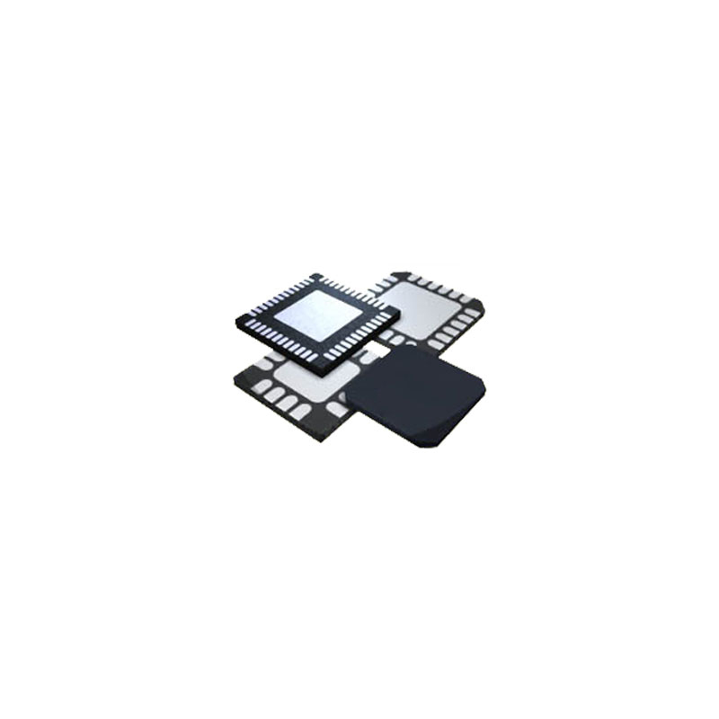
40-VFQFNExposedPadManufacturer:
Renesas Electronics Corporation
Mfr.Part #:
840N202CKI-000LFT
Datasheet:
Series:
FemtoClock® NG
Programmabe:
Not Verified
PLL:
Yes with Bypass
Input:
HCSL, LVDS, LVHSTL, LVPECL, Crystal
EDA/CAD Models:
Please fill in the short form below and we will provide you the quotation immediately.
The 840N202I is a highly flexible FemtoClock® NG general purpose, low phase noise Frequency Translator / Synthesizer with alarm and monitoring functions suitable for networking and communications applications. It is able to generate any output frequency in the 1MHz - 250MHz range (see Table 3 for details). A wide range of input reference clocks and a range of low- cost fundamental mode crystal frequencies may be used as the source for the output frequency. The 840N202I has three operating modes to support a very broad spectrum of applications: Frequency Synthesizer , High-Bandwidth Frequency Translator and a Low-Bandwidth Frequency Translator.
This device provides two factory-programmed default power-up configurations burned into One-Time Programmable (OTP) memory. The configuration to be used is selected by the CONFIG pin. The two configurations are specified by the customer and are programmed by IDT during the final test phase from an on-hand stock of blank devices. The two configurations may be completely independent of one another.
To see other devices in this product family, visit the Universal Frequency Translators page.
| Series | FemtoClock® NG | Programmabe | Not Verified |
| PLL | Yes with Bypass | Input | HCSL, LVDS, LVHSTL, LVPECL, Crystal |
| Output | LVCMOS, LVTTL | Number of Circuits | 1 |
| Ratio - Input:Output | 3:2 | Differential - Input:Output | Yes/No |
| Frequency - Max | 250MHz | Divider/Multiplier | Yes/No |
| Voltage - Supply | 2.375V ~ 3.465V | Operating Temperature | -40°C ~ 85°C |
| Mounting Type | Surface Mount | Base Product Number | 840N202 |
After-Sales & Settlement Related
 Payment
Payment Method


For alternative payment channels, please reach out to us at:
[email protected] Shipping & Packing
Shipping Method


AVAQ determines and packages all devices based on electrostatic discharge (ESD) and moisture sensitivity level (MSL) protection requirements.
 Warranty

365-Day Product
Quality Guarantee
We promise to provide 365 days quality assurance service for all our products.
| Qty. | Unit Price | Ext. Price |
|---|---|---|
| 1+ | - | - |
The prices below are for reference only.
All bill of materials (BOM) can be sent via email to ![]() [email protected],
or fill below form to Quote for 840N202CKI-000LFT, guaranteed quotes back within
[email protected],
or fill below form to Quote for 840N202CKI-000LFT, guaranteed quotes back within
![]() 12hr.
12hr.

SI5341B-D-GM
SILICON
1040+ $5.980

AK1573
Asahi Kasei Microdevices/AKM
1000+ $2.489

MN3102
Panasonic
Consumer Circuit, MOS, PDIP8, 0.300 INCH, PLASTIC, DIP-8

SI5351A-B-GT
Skyworks
Clock Generator Si5351A-B-GT PK

LMX2594RHAT
Texas Instruments
15-GHz wideband PLLatinum™ RF synthesizer with phase synchronization and JESD204B support 40-VQFN -40 to 85"