Payment Method


Digital Signal Processors & Controllers - DSP, DSC C2000 military 32-bit MCU with 150-MHz, 256-kb Flash, EMIF 172-CFP -55 to 125
Manufacturer:
Mfr.Part #:
5962-0620801QXC
Datasheet:
Series:
*
CPU:
C28x
Frequency (MHz):
150
Flash memory (kByte):
256
Please fill in the short form below and we will provide you the quotation immediately.
The SM320F2812 device, member of the C28x DSP generation, is a highly integrated, high-performance solution for demanding control applications. The functional blocks and the memory maps are described in Section 3, Functional Overview.
Throughout this document, SM320F2812 is abbreviated as F2812.
TMS320C24x, Code Composer Studio, DSP/BIOS, and MicroStar BGA are trademarks of Texas Instruments.
IEEE Standard 1149.1-1990, IEEE Standard Test-Access Port
TMS320C28x is a trademark of Texas Instruments.
All trademarks are the property of their respective owners.
| Category | Integrated Circuits (ICs)EmbeddedDSP (Digital Signal Processors) | Series | * |
| CPU | C28x | Frequency (MHz) | 150 |
| Flash memory (kByte) | 256 | RAM (kByte) | 36 |
| ADC resolution (Bps) | 12 | Total processing (MIPS) | 150 |
| Features | 2-pin oscillator, 32-bit CPU timers, External memory interface, McBSP, Watchdog timer | UART | 2 |
| CAN (#) | 1 | PWM (Ch) | 16 |
| Number of ADC channels | 16 | Direct memory access (Ch) | 0 |
| SPI | 1 | QEP | 2 |
| Operating temperature range (°C) | -55 to 125 | Rating | Military |
| Communication interface | CAN, McBSP, SPI, UART |
After-Sales & Settlement Related
 Payment
Payment Method


For alternative payment channels, please reach out to us at:
[email protected] Shipping & Packing
Shipping Method


AVAQ determines and packages all devices based on electrostatic discharge (ESD) and moisture sensitivity level (MSL) protection requirements.
 Warranty

365-Day Product
Quality Guarantee
We promise to provide 365 days quality assurance service for all our products.
| Qty. | Unit Price | Ext. Price |
|---|---|---|
| 1+ | - | - |
The prices below are for reference only.
All bill of materials (BOM) can be sent via email to ![]() [email protected],
or fill below form to Quote for 5962-0620801QXC, guaranteed quotes back within
[email protected],
or fill below form to Quote for 5962-0620801QXC, guaranteed quotes back within
![]() 12hr.
12hr.
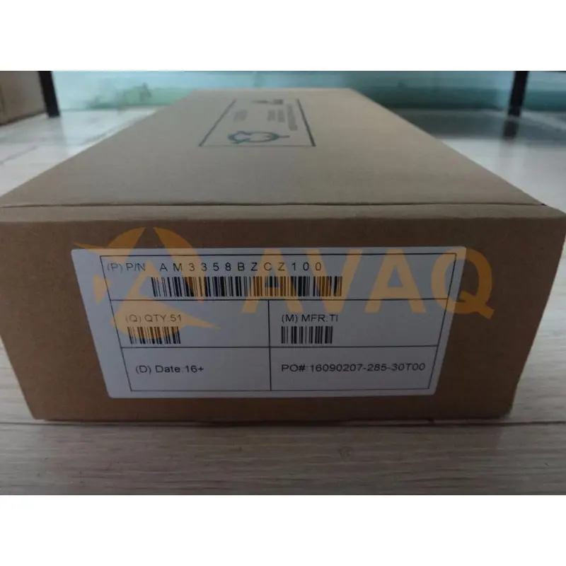
AM3358BZCZ100
TI
126+ $8.358
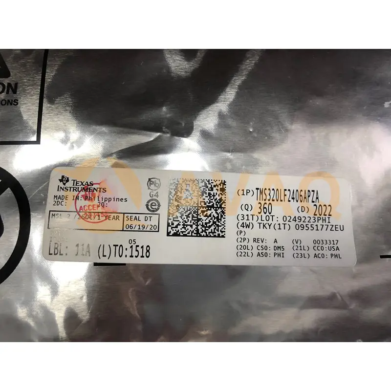
TMS320LF2406APZA
Texas Instruments
100+ $7.554
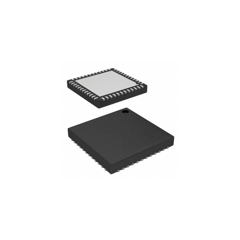
MSP430FR5969
TI
16 MHz MCU with 64KB FRAM, 2KB SRAM, AES, 12-bit ADC, comparator, DMA, UART/SPI/I2C, timer
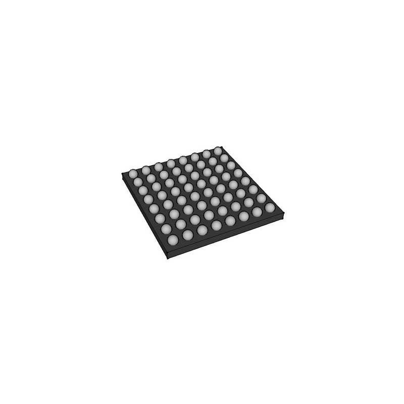
TMS320C6713
TI
FLOATING-POINTDIGITALSIGNALPROCESSORS
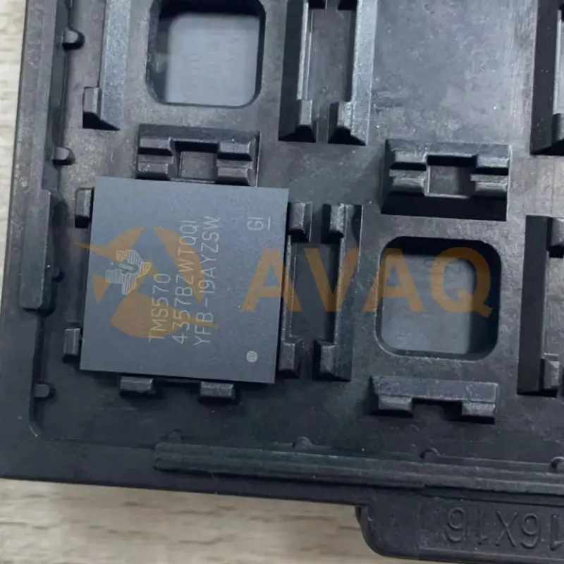
TMS5704357BZWTQQ1
Texas Instruments, Inc
MCU 32-bit ARM Cortex R5F RISC 4MB Flash 1.2V/3.3V Automotive 337-Pin NFBGA Tray

Delivery in 20 days.