Payment Method


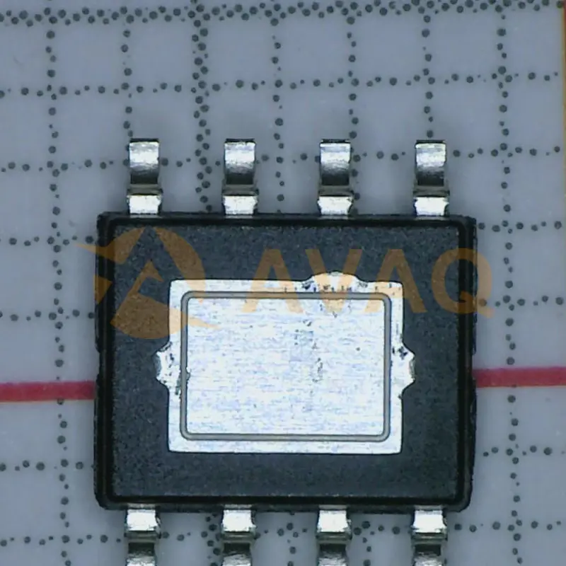
Automotive 3-A, 120-V half bridge gate driver with 8-V UVLO and negative voltage handling
SOP-8Manufacturer:
Mfr.Part #:
UCC27201AQDDARQ1
Datasheet:
Bus voltage (max) (V):
110
Power switch:
MOSFET
Input VCC (min) (V):
8
Input VCC (max) (V):
17
EDA/CAD Models:
Please fill in the short form below and we will provide you the quotation immediately.
The UCC27201A-Q1 high frequency N-Channel MOSFET driver includes a 120-V bootstrap diode and high-side/low-side driver with independent inputs for maximum control flexibility. This allows for N-Channel MOSFET control in half-bridge, full-bridge, two-switch forward and active clamp forward converters. The low-side and the high-side gate drivers are independently controlled and matched to 1-ns between the turn-on and turn-off of each other. The UCC27201A-Q1 is based on the popular UCC27200 and UCC27201 drivers, but offer some enhancements. In order to improve performance in noisy power supply environments the UCC27201A-Q1 has the ability to withstand a maximum of -18 V on its HS pin.
An on-chip bootstrap diode eliminates the external discrete diodes. Under-voltage lockout is provided for both the high-side and the low-side drivers forcing the outputs low if the drive voltage is below the specified threshold.
The UCC27201A-Q1 has TTL-compatible thresholds and is offered in a 10-Pin VSON and an 8-pin SOIC with a thermal pad.
For all available packages, see the orderable addendum at the end of the data sheet.| Bus voltage (max) (V) | 110 | Power switch | MOSFET |
| Input VCC (min) (V) | 8 | Input VCC (max) (V) | 17 |
| Peak output current (A) | 3 | Operating temperature range (°C) | -40 to 125 |
| Undervoltage lockout (typ) (V) | 8 | Rating | Automotive |
| Propagation delay time (µs) | 0.02 | Rise time (ns) | 8 |
| Fall time (ns) | 7 | Iq (mA) | 0.001 |
| Input threshold | TTL | Channel input logic | TTL |
| Negative voltage handling at HS pin (V) | -15 | Features | Negative voltage handling |
| Driver configuration | Noninverting |
After-Sales & Settlement Related
 Payment
Payment Method


For alternative payment channels, please reach out to us at:
[email protected] Shipping & Packing
Shipping Method


AVAQ determines and packages all devices based on electrostatic discharge (ESD) and moisture sensitivity level (MSL) protection requirements.
 Warranty

365-Day Product
Quality Guarantee
We promise to provide 365 days quality assurance service for all our products.
| Qty. | Unit Price | Ext. Price |
|---|---|---|
| 1+ | - | - |
The prices below are for reference only.
All bill of materials (BOM) can be sent via email to ![]() [email protected],
or fill below form to Quote for UCC27201AQDDARQ1, guaranteed quotes back within
[email protected],
or fill below form to Quote for UCC27201AQDDARQ1, guaranteed quotes back within
![]() 12hr.
12hr.

Delivered in a month. Thank you!