Payment Method


167-MHz, LVCMOS, programmable 3-PLL clock synthesizer / multiplier / divider
Manufacturer: Texas Instruments, Inc
Mfr.Part #: CDCE906PW
Datasheet:
CDCE906PW Datasheet (PDF)
![]()
Package/Case: TSSOP20
Product Type: Clock & Timer ICs
RoHS:
Lifecycle: Active
EDA/CAD Models:
![]() Request Free CAD Models for CDCE906PW
Request Free CAD Models for CDCE906PW
Please fill in the short form below and we will provide you the quotation immediately.
The CDCE906 is one of the smallest and powerful PLL synthesizer / multiplier / divider available today. Despite its small physical outlines, the CDCE906 is flexible. It has the capability to produce an almost independent output frequency from a given input frequency.
The input frequency can be derived from a LVCMOS, differential input clock, or a single crystal. The appropriate input waveform can be selected via the SMBus data interface controller.
To achieve an independent output frequency the reference divider M and the feedback divider N for each PLL can be set to values from 1 up to 511 for the M-Divider and from 1 up to 4095 for the N-Divider. The PLL-VCO (voltage controlled oscillator) frequency than is routed to the free programmable output switching matrix to any of the six outputs. The switching matrix includes an additional 7-bit post-divider (1-to-127) and an inverting logic for each output.
The deep M/N divider ratio allows the generation of zero ppm clocks from any reference input frequency (e.g., a 27 MHz).
The CDCE906 includes three PLLs of those one supports SSC (spread-spectrum clocking). PLL1, PLL2, and PLL3 are designed for frequencies up to 167 MHz and optimized for zero-ppm applications with wide divider factors.
PLL2 also supports center-spread and down-spread spectrum clocking (SSC). This is a common technique to reduce electro-magnetic interference. Also, the slew-rate controllable (SRC) output edges minimize EMI noise.
Based on the PLL frequency and the divider settings, the internal loop filter components will be automatically adjusted to achieve high stability and optimized jitter transfer characteristic of the PLL.
The device supports non-volatile EEPROM programming for easy-customized application. It is preprogrammed with a factory default configuration (see Figure 13) and can be reprogrammed to a different application configuration before it goes onto the PCB or reprogrammed by in-system programming. A different device setting is programmed via the serial SMBus interface.
Two free programmable inputs, S0 and S1, can be used to control for each application the most demanding logic control settings (outputs disable to low, outputs 3-state, power down, PLL bypass, etc).
The CDCE906 has three power supply pins, VCC, VCCOUT1 and VCCOUT2. VCC is the power supply for the device. It operates from a single 3.3-V supply voltage. VCCOUT1 and VCCOUT2 are the power supply pins for the outputs. VCCOUT1 supplies the outputs Y0 and Y1 and VCCOUT2 supplies the outputs Y2, Y3, Y4, and Y5. Both outputs supplies can be 2.3 V to 3.6 V. At output voltages lower than 3.3 V, the output drive current is limited.
The CDCE906 is characterized for operation from 0°C to 70°C.

Pro-Clock is a trademark of Texas Instruments.


| Category | Integrated Circuits (ICs)Clock/TimingClock Generators, PLLs, Frequency Synthesizers | Mfr | Texas Instruments |
| Series | - | Package | Tube |
| Product Status | Active | Digi-Key Programmable | Verified |
| Type | PLL Frequency Synthesizer | PLL | Yes with Bypass |
| Input | LVCMOS, Crystal | Output | LVCMOS |
| Number of Circuits | 1 | Ratio - Input:Output | 1:6 |
| Differential - Input:Output | Yes/No | Frequency - Max | 167MHz |
| Divider/Multiplier | Yes/Yes | Voltage - Supply | 3V ~ 3.6V |
| Operating Temperature | 0°C ~ 70°C | Mounting Type | Surface Mount |
| Package / Case | 20-TSSOP (0.173", 4.40mm Width) | Supplier Device Package | 20-TSSOP |
| Base Product Number | CDCE906 |
After-Sales & Settlement Related
 Payment
Payment Method


For alternative payment channels, please reach out to us at:
[email protected] Shipping & Packing
Shipping Method


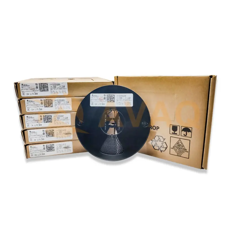
AVAQ determines and packages all devices based on electrostatic discharge (ESD) and moisture sensitivity level (MSL) protection requirements.
 Warranty

365-Day Product
Quality Guarantee
We promise to provide 365 days quality assurance service for all our products.
| Qty. | Unit Price | Ext. Price |
|---|---|---|
| 1+ | - | - |
The prices below are for reference only.
All bill of materials (BOM) can be sent via email to ![]() [email protected], or fill below form to Quote for CDCE906PW, guaranteed quotes back within
[email protected], or fill below form to Quote for CDCE906PW, guaranteed quotes back within
![]() 12hr.
12hr.
Everything works, great thing