This website uses cookies. By using this site, you consent to the use of cookies. For more information, please take a look at our Privacy Policy.

TMS320DM6467TCUT9 +BOM

Digital Media System-on-Chip

  • Manufacturer:

    Texas Instruments, Inc

  • Mfr.Part #:

    TMS320DM6467TCUT9

  • Datasheet:

    TMS320DM6467TCUT9 Datasheet (PDF) pdf-icon

  • Series:

    TMS320DM646x, DaVinci™

  • Type:

    Digital Media System-on-Chip (DMSoC)

  • Interface:

    EBI/EMI, Ethernet, HPI, I²C, McASP, PCI, SPI, UART, USB

  • Non-Volatile Memory:

    ROM (8kB)

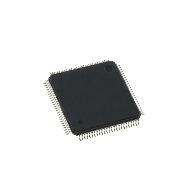
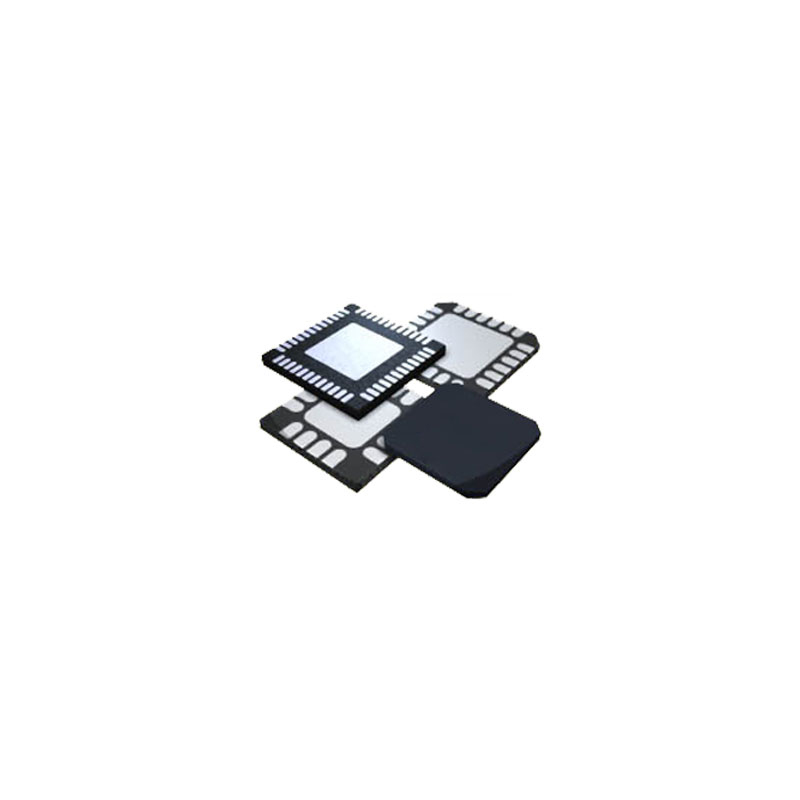
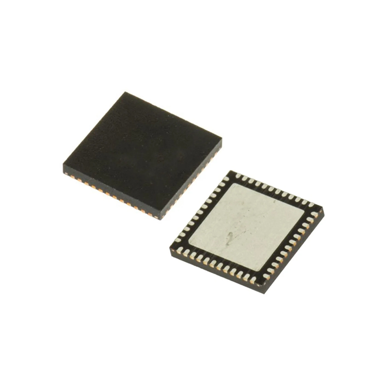
TMS320DM6467TCUT9 General Description

The TMS320DM6467T (also referenced as DM6467T) leverages TI's DaVinci™ technology to meet the networked media encode and decode application processing needs of next-generation embedded devices.

The DM6467T enables OEMs and ODMs to quickly bring to market devices featuring robust operating systems support, rich user interfaces, high processing performance, and long battery life through the maximum flexibility of a fully integrated mixed processor solution.

The dual-core architecture of the DM6467T provides benefits of both DSP and Reduced Instruction Set Computer (RISC) technologies, incorporating a high-performance TMS320C64x+ DSP core and an ARM926EJ-S core.

The ARM926EJ-S is a 32-bit RISC processor core that performs 32-bit or 16-bit instructions and processes 32-bit, 16-bit, or 8-bit data. The core uses pipelining so that all parts of the processor and memory system can operate continuously.

The ARM core incorporates:

  • A coprocessor 15 (CP15) and protection module
  • Data and program Memory Management Units (MMUs) with table look-aside buffers.
  • Separate 16K-byte instruction and 8K-byte data caches. Both are four-way associative with virtual index virtual tag (VIVT).

The TMS320C64x+™ DSPs are the highest-performance fixed-point DSP generation in the TMS320C6000™ DSP platform. It is based on an enhanced version of the second-generation high-performance, advanced very-long-instruction-word (VLIW) architecture developed by Texas Instruments (TI), making these DSP cores an excellent choice for digital media applications. The C64x is a code-compatible member of the C6000™ DSP platform. The TMS320C64x+ DSP is an enhancement of the C64x+ DSP with added functionality and an expanded instruction set.

Any reference to the C64x DSP or C64x CPU also applies, unless otherwise noted, to the C64x+ DSP and C64x+ CPU, respectively.

With performance of up to 8000 million instructions per second (MIPS) at a clock rate of 1 GHz, the C64x+ core offers solutions to high-performance DSP programming challenges. The DSP core possesses the operational flexibility of high-speed controllers and the numerical capability of array processors. The C64x+ DSP core processor has 64 general-purpose registers of 32-bit word length and eight highly independent functional units— two multipliers for a 32-bit result and six arithmetic logic units (ALUs). The eight functional units include instructions to accelerate the performance in video and imaging applications. The DSP core can produce four 16-bit multiply-accumulates (MACs) per cycle for a total of 4000 million MACs per second (MMACS), or eight 8-bit MACs per cycle for a total of 8000 MMACS. For more details on the C64x+ DSP, see the TMS320C64x/C64x+ DSP CPU and Instruction Set Reference Guide (literature number SPRU732).

The DM6467T also has application-specific hardware logic, on-chip memory, and additional on-chip peripherals similar to the other C6000 DSP platform devices. The DM6467T core uses a two-level cache-based architecture. The Level 1 program cache (L1P) is a 256K-bit direct mapped cache and the Level 1 data cache (L1D) is a 640K-bit 2-way set-associative cache. The Level 2 memory/cache (L2) consists of an 512K-bit memory space that is shared between program and data space. L2 memory can be configured as mapped memory, cache, or combinations of the two.

The peripheral set includes: a configurable video port; a 10/100/1000 Mb/s Ethernet MAC (EMAC) with a Management Data Input/Output (MDIO) module; a 4-bit transfer/4-bit receive VLYNQ interface; an inter-integrated circuit (I2C) Bus interface; a multichannel audio serial port (McASP0) with 4 serializers; a secondary multichannel audio serial port (McASP1) with a single transmit serializer; 2 64-bit general-purpose timers each configurable as 2 independent 32-bit timers; 1 64-bit watchdog timer; a configurable 32-bit host port interface (HPI); up to 33-pins of general-purpose input/output (GPIO) with programmable interrupt/event generation modes, multiplexed with other peripherals; 3 UART/IrDA/CIR interfaces with modem interface signals on UART0; 2 pulse width modulator (PWM) peripherals; an ATA/ATAPI-6 interface; a 66-MHz peripheral component interface (PCI); and 2 external memory interfaces: an asynchronous external memory interface (EMIFA) for slower memories/peripherals, and a higher speed synchronous memory interface for DDR2.

The Ethernet Media Access Controller (EMAC) provides an efficient interface between the DM6467T and the network. The DM6467T EMAC support both 10Base-T and 100Base-TX, or 10 Mbits/second (Mbps) and 100 Mbps in either half- or full-duplex mode; and 1000Base-TX (1 Gbps) in full-duplex mode with hardware flow control and quality of service (QOS) support.

The Management Data Input/Output (MDIO) module continuously polls all 32 MDIO addresses in order to enumerate all PHY devices in the system. Once a PHY candidate has been selected by the ARM, the MDIO module transparently monitors its link state by reading the PHY status register. Link change events are stored in the MDIO module and can optionally interrupt the ARM, allowing the ARM to poll the link status of the device without continuously performing costly MDIO accesses.

The PCI, HPI, I2C, SPI, USB2.0, and VLYNQ ports allow the DM6467T to easily control peripheral devices and/or communicate with host processors.

The DM6467T also includes a High-Definition Video/Imaging Co-processor (HDVICP) and Video Data Conversion Engine (VDCE) to offload many video and imaging processing tasks from the DSP core, making more DSP MIPS available for common video and imaging algorithms. For more information on the HDVICP enhanced codecs, such as H.264 and MPEG4, please contact your nearest TI sales representative.

The rich peripheral set provides the ability to control external peripheral devices and communicate with external processors. For details on each of the peripherals, see the related sections later in this document and the associated peripheral reference guides.

The DM6467T has a complete set of development tools for both the ARM and DSP. These include C compilers, a DSP assembly optimizer to simplify programming and scheduling, and a Windows™ debugger interface for visibility into source code execution.

Texas Instruments, Inc Inventory

Key Features

  • High-Performance Digital Media SoC
    • 1-GHz C64x+™ Clock Rate
    • 500-MHz ARM926EJ-S™ Clock Rate
    • Eight 32-Bit C64x+ Instructions/Cycle
    • 8000 C64x+ MIPS
    • Fully Software-Compatible With C64x / ARM9™
    • Industrial Temperature Devices Available
  • Advanced Very-Long-Instruction-Word (VLIW) TMS320C64x+™ DSP Core
    • Eight Highly Independent Functional Units
      • Six ALUs (32-/40-Bit), Each Supports Single 32-Bit, Dual 16-Bit, or Quad 8-Bit Arithmetic per Clock Cycle
      • Two Multipliers Support Four 16 x 16-Bit Multiplies (32-Bit Results) per Clock Cycle or Eight 8 x 8-Bit Multiplies (16-Bit Results) per Clock Cycle
    • Load-Store Architecture With Non-Aligned Support
    • 64 32-Bit General-Purpose Registers
    • Instruction Packing Reduces Code Size
    • All Instructions Conditional
    • Additional C64x+™ Enhancements
      • Protected Mode Operation Exceptions
      • Support for Error Detection and Program Redirection
      • Hardware Support for Modulo Loop Operation
  • C64x+ Instruction Set Features
    • Byte-Addressable (8-/16-/32-/64-Bit Data)
    • 8-Bit Overflow Protection
    • Bit-Field Extract, Set, Clear
    • Normalization, Saturation, Bit-Counting
    • Compact 16-Bit Instructions
    • Additional Instructions to Support Complex Multiplies
  • C64x+ L1/L2 Memory Architecture
    • 32K-Byte L1P Program RAM/Cache (Direct Mapped)
    • 32K-Byte L1D Data RAM/Cache (2-Way Set-Associative)
    • 128K-Byte L2 Unified Mapped RAM/Cache (Flexible RAM/Cache Allocation)
  • ARM926EJ-S Core
    • Support for 32-Bit and 16-Bit (Thumb® Mode) Instruction Sets
    • DSP Instruction Extensions and Single Cycle MAC
    • ARM® Jazelle® Technology
    • EmbeddedICE-RT™ Logic for Real-Time Debug
  • ARM9 Memory Architecture
    • 16K-Byte Instruction Cache
    • 8K-Byte Data Cache
    • 32K-Byte RAM
    • 8K-Byte ROM
  • Embedded Trace Buffer™ (ETB11™) With 4KB Memory for ARM9 Debug
  • Endianness: Little Endian for ARM and DSP
  • Dual Programmable High-Definition Video Image Co-Processor (HDVICP) Engines
    • Supports a Range of Encode, Decode, and Transcode Operations
      • H.264, MPEG2, VC1, MPEG4 SP/ASP
  • 150-MHz Video Port Interface (VPIF)
    • Two 8-Bit SD (BT.656), Single 16-Bit HD (BT.1120), or Single Raw (8-/10-/12-Bit) Video Capture Channels
    • Two 8-Bit SD (BT.656) or Single 16-Bit HD (BT.1120) Video Display Channels
  • Video Data Conversion Engine (VDCE)
    • Horizontal and Vertical Downscaling
    • Chroma Conversion (4:2:2 ↔ 4:2:0)
  • Two Transport Stream Interface (TSIF) Modules (One Parallel/Serial and One Serial Only)
    • TSIF for MPEG Transport Stream
    • Simultaneous Synchronous or Asynchronous Input/Output Streams
    • Absolute Time Stamp Detection
    • PID Filter With 7 PID Filter Tables
    • Corresponding Clock Reference Generator (CRGEN) Modules for System Time-Clock Recovery
  • External Memory Interfaces (EMIFs)
    • Up to 400-MHz 32-Bit DDR2 SDRAM Memory Controller With 512M-Byte Address Space (1.8-V I/O)
    • Asynchronous16-Bit Wide EMIF (EMIFA) With 128M-Byte Address Reach
      • Flash Memory Interfaces
        • NOR (8-/16-Bit-Wide Data)
        • NAND (8-/16-Bit-Wide Data)
  • Enhanced Direct-Memory-Access (EDMA) Controller (64 Independent Channels)
    • Programmable Default Burst Size
  • 10/100/1000 Mb/s Ethernet MAC (EMAC)
    • IEEE 802.3 Compliant (3.3-V I/O Only)
    • Supports MII and GMII Media Independent Interfaces
    • Management Data I/O (MDIO) Module
  • USB Port With Integrated 2.0 PHY
    • USB 2.0 High-/Full-Speed Client
    • USB 2.0 High-/Full-/Low-Speed Host (Mini-Host, Supporting One External Device)
  • 32-Bit, 66-MHz, 3.3 V Peripheral Component Interconnect (PCI) Master/Slave Interface
    • Conforms to PCI Specification 2.3
  • Two 64-Bit General-Purpose Timers (Each Configurable as Two 32-Bit Timers)
  • One 64-Bit Watch Dog Timer
  • Three Configurable UART/IrDA/CIR Modules
    (One With Modem Control Signals)
    • Supports up to 1.8432 Mbps UART
    • SIR and MIR (0.576 MBAUD)
    • CIR With Programmable Data Encoding
  • One Serial Peripheral Interface (SPI) With Two Chip-Selects
  • Master/Slave Inter-Integrated Circuit (I2C Bus™)
  • Two Multichannel Audio Serial Ports (McASPs)
    • One Four Serializer Transmit/Receive Port
    • One Single DIT Transmit Port for S/PDIF
  • 32-Bit Host Port Interface (HPI)
  • VLYNQ™ Interface (FPGA Interface)
  • Two Pulse Width Modulator (PWM) Outputs
  • ATA/ATAPI I/F (ATA/ATAPI-6 Specification)
  • Up to 33 General-Purpose I/O (GPIO) Pins (Multiplexed With Other Device Functions)
  • On-Chip ARM ROM Bootloader (RBL)
  • Individual Power-Saving Modes for ARM/DSP
  • Flexible PLL Clock Generators
  • IEEE-1149.1 (JTAG) Boundary-Scan-Compatible
  • 529-Pin Pb-Free BGA Package (CUT Suffix), 0.8-mm Ball Pitch
  • 0.09-µm/7-Level Cu Metal Process (CMOS)
  • 3.3-V and 1.8-V I/O, 1.3-V Internal
  • Community Reesources
    • TI E2E Community
    • TI Embedded Processors Wiki

All other trademarks are the property of their respective owners.

Applications:
  • Video Encode/Decode/Transcode/Transrate
  • Digital Media
  • Networked Media Encode/Decode
  • Video Imaging
  • Video Infrastructure
  • Video Conferencing
Texas Instruments, Inc Original Stock
Texas Instruments, Inc Inventory

Specifications

Category Integrated Circuits (ICs)EmbeddedDSP (Digital Signal Processors) Series TMS320DM646x, DaVinci™
Type Digital Media System-on-Chip (DMSoC) Interface EBI/EMI, Ethernet, HPI, I²C, McASP, PCI, SPI, UART, USB
Clock Rate - Non-Volatile Memory ROM (8kB)
On-Chip RAM 248kB Voltage - I/O 1.8V, 3.3V
Voltage - Core 1.30V Operating Temperature 0°C ~ 85°C (TC)
Mounting Type Surface Mount Base Product Number TMS320

Service Policies and Others

After-Sales & Settlement Related

payment Payment

Payment Method

hsbc
TT/Wire Transfer
paypal
Paypal
wu
Western Union
mg
Money Gram

For alternative payment channels, please reach out to us at:

[email protected]
shipping Shipping & Packing

Shipping Method

fedex
Fedex
ups
UPS
dhl
DHL
tnt
NTN
Packing

AVAQ determines and packages all devices based on electrostatic discharge (ESD) and moisture sensitivity level (MSL) protection requirements.

Warranty Warranty

We promise to provide 365 days quality assurance service for all our products.

Reviews

You need to log in to reply. Sign In | Sign Up

In Stock: 5,522

Minimum Order: 1

Qty. Unit Price Ext. Price
1+ $350.183 $350.18
200+ $135.517 $27,103.40
500+ $130.754 $65,377.00
1000+ $128.401 $128,401.00

The prices below are for reference only.