This website uses cookies. By using this site, you consent to the use of cookies. For more information, please take a look at our Privacy Policy.

TLC555QDRQ1 +BOM

Automotive LinCMOS TIMER

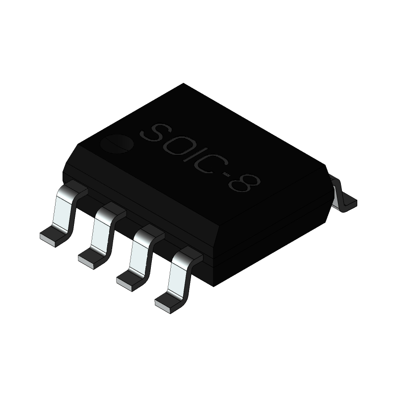
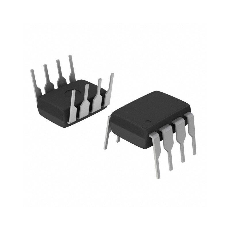
TLC555QDRQ1 General Description

The TLC555-Q1 is a monolithic timing circuit fabricated using the TI LinCMOS™ process. The timer is fully compatible with CMOS, TTL, and MOS logic and operates at frequencies up to 2 MHz. Because of its high input impedance, this device uses smaller timing capacitors than those used by the NE555. As a result, more accurate time delays and oscillations are possible. Power consumption is low across the full range of power-supply voltage.

Like the NE555, the TLC555-Q1 has a trigger level equal to approximately one-third of the supply voltage and a threshold level equal to approximately two-thirds of the supply voltage. These levels can be altered by use of the control voltage terminal (CONT).

When the trigger input (TRIG) falling below the trigger level sets the flip-flop, and the output goes high. Having TRIG above the trigger level and the threshold input (THRES) above the threshold level resets the flip-flop, and the output is low. The reset input (RESET) can override all other inputs, and a possible use is to initiate a new timing cycle. RESET going low resets the flip-flop, and the output is low. Whenever the output is low, a low-impedance path exists between the discharge terminal (DISCH) and GND. Tie all unused inputs to an appropriate logic level to prevent false triggering.

The advantage of the TLC555-Q1 is that it exhibits greatly reduced supply-current spikes during output transitions. Although the CMOS output is capable of sinking over 100 mA and sourcing over 10 mA, the main reason the TLC555-Q1 is able to have low current spikes is due to its edge rates. This minimizes the need for the large decoupling capacitors required by the NE555.

The TLC555-Q1 is characterized for operation over the full automotive temperature range of –40°C to 125°C.

TI Inventory

Key Features

  • Qualified for Automotive Applications
  • Very Low Power Consumption
    • 1 mW (Typical) at VDD = 5 V
  • Capable of Operation in Astable Mode
  • CMOS Output Capable of Swinging Rail to Rail
  • High-Output-Current Capability
    • Sink 100 mA (Typical)
    • Source 10 mA (Typical)
  • Output Fully Compatible With CMOS, TTL, and
    MOS
  • Low Supply Current Reduces Spikes During
    Output Transitions
  • Single-Supply Operation From 2 V to 15 V
  • Functionally Interchangeable With the NE555;
    Has Same Pinout
TI Original Stock
TI Inventory

Specifications

Function General-purpose timer Iq (typ) (mA) 0.17
Rating Automotive Operating temperature range (°C) -40 to 125
Supply voltage (max) (V) 15 Supply voltage (min) (V) 2
TI functional safety category Functional Safety-Capable

Service Policies and Others

After-Sales & Settlement Related

payment Payment

Payment Method

hsbc
TT/Wire Transfer
paypal
Paypal
wu
Western Union
mg
Money Gram

For alternative payment channels, please reach out to us at:

[email protected]
shipping Shipping & Packing

Shipping Method

fedex
Fedex
ups
UPS
dhl
DHL
tnt
NTN
Packing

AVAQ determines and packages all devices based on electrostatic discharge (ESD) and moisture sensitivity level (MSL) protection requirements.

Warranty Warranty

We promise to provide 365 days quality assurance service for all our products.

Ratings and Reviews

More
Z
Z**e 01/20/2023

parcel arrived quickly and as described

13
D
D**n 10/24/2022

Came pritty soon. Not tested yet.

16
M
M**n 01/29/2022

Ordinary ribbon cable. Good for servo extenders, etc.

4
C
C**n 12/14/2021

The goods went to moscow about 5 days. Packed all well. I haven't checked in yet.

11

Reviews

You need to log in to reply. Sign In | Sign Up

TLC555QDRQ1 Datasheet PDF

Preliminary Specification TLC555QDRQ1 PDF Download

TLC555QDRQ1 PDF Preview

In Stock: 4,837

Minimum Order: 1

Qty. Unit Price Ext. Price
1+ - -

The prices below are for reference only.