Payment Method


Dual 4-port LVDS repeater
Manufacturer:
Mfr.Part #:
SN65LVDS109DBT
Datasheet:
Function:
Driver, Repeater
Protocols:
LVDS
Number of transmitters:
8
Number of receivers:
2
EDA/CAD Models:
Please fill in the short form below and we will provide you the quotation immediately.
The SN65LVDS109 and SN65LVDS117 are configured as two identical banks, each bank having one differential line receiver connected to either four ('109) or eight ('117) differential line drivers. The outputs are arranged in pairs having one output from each of the two banks. Individual output enables are provided for each pair of outputs and an additional enable is provided for all outputs.
The line receivers and line drivers implement the electrical characteristics of low-voltage differential signaling (LVDS). LVDS, as specified in EIA/TIA-644, is a data signaling technique that offers low power, low noise emission, high noise immunity, and high switching speeds. (Note: The ultimate rate and distance of data transfer is dependent upon the attenuation characteristics of the media, the noise coupling to the environment, and other system characteristics.)
The intended application of these devices, and the LVDS signaling technique, is for point-to-point or point-to-multipoint (distributed simplex) baseband data transmission on controlled impedance media of approximately 100 Ω. The transmission media may be printed-circuit board traces, backplanes, or cables. The large number of drivers integrated into the same silicon substrate, along with the low pulse skew of balanced signaling, provides extremely precise timing alignment of the signals being repeated from the inputs. This is particularly advantageous for implementing system clock and data distribution trees.
The SN65LVDS109 and SN65LVDS117 are characterized for operation from –40°C to 85°C.
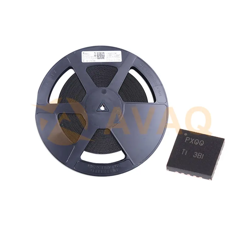
| Function | Driver, Repeater | Protocols | LVDS |
| Number of transmitters | 8 | Number of receivers | 2 |
| Supply voltage (V) | 3.3 | Signaling rate (MBits) | 400 |
| Input signal | LVDS | Output signal | BTL, CTT, GTL, HSTL, LVCMOS, LVDS, LVPECL, LVTTL, PECL, SSTL |
| Rating | Catalog | Operating temperature range (°C) | -40 to 85 |
| feature-function | Driver/Receiver | feature-number-of-drivers | 8 |
| feature-number-of-receivers | 2 | feature-number-of-elements-per-chip | 2 |
| feature-transmission-data-rate-mbps | 400 | feature-maximum-propagation-delay-time-ns | 4.5 |
| feature-input-signal-type | LVDS | feature-differential-input-low-threshold-voltage-v | -0.1 |
| feature-differential-input-high-threshold-voltage-v | 0.1 | feature-maximum-differential-output-voltage-v | 0.454 |
| feature-maximum-input-current-ua | 20 | feature-supplier-temperature-grade | |
| feature-packaging | Tube | feature-rad-hard | |
| feature-pin-count | 38 | feature-cecc-qualified | No |
| feature-esd-protection | feature-escc-qualified | ||
| feature-military | No | feature-aec-qualified | No |
| feature-aec-qualified-number | feature-eccn-code | EAR99 | |
| feature-svhc | Yes | feature-svhc-exceeds-threshold | No |
After-Sales & Settlement Related
 Payment
Payment Method


For alternative payment channels, please reach out to us at:
[email protected] Shipping & Packing
Shipping Method


AVAQ determines and packages all devices based on electrostatic discharge (ESD) and moisture sensitivity level (MSL) protection requirements.
 Warranty

365-Day Product
Quality Guarantee
We promise to provide 365 days quality assurance service for all our products.
| Qty. | Unit Price | Ext. Price |
|---|---|---|
| 1+ | - | - |
The prices below are for reference only.
All bill of materials (BOM) can be sent via email to ![]() [email protected],
or fill below form to Quote for SN65LVDS109DBT, guaranteed quotes back within
[email protected],
or fill below form to Quote for SN65LVDS109DBT, guaranteed quotes back within
![]() 12hr.
12hr.
SN65HVD230DR
TI
1000+ $0.403
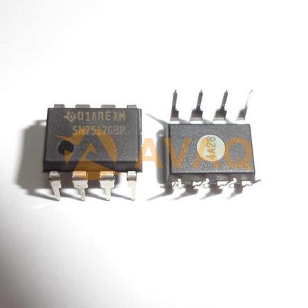
SN75176BP
Texas Instruments
1000+ $0.309

PCF8574AN
TI
8-bit 2.5- to 5.5-V I2C/SMBus I/O expander with interrupt
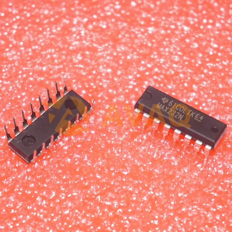
MAX232N
Texas Instruments
Dual Transmitter/Receiver RS-232 16-Pin PDIP Tube
TCA6424RGJR
Texas Instruments, Inc
24-bit translating 1.65- to 5.5-V I2C/SMBus I/O expander with interrupt, reset & config registers