Payment Method


2-bit bidirectional 2.3- to 3.6-V 400-kHz I2C/SMBus buffer
Manufacturer:
Mfr.Part #:
PCA9515ADGKR
Datasheet:
Type:
Buffer, ReDriver
Applications:
I²C
Input:
2-Wire Bus
Output:
2-Wire Bus
EDA/CAD Models:
Please fill in the short form below and we will provide you the quotation immediately.
This dual bidirectional I2C buffer is operational at 2.3-V to 3.6-V VCC.
The PCA9515A is a BiCMOS integrated circuit intended for I2C bus and SMBus systems applications. The device contains two identical bidirectional open-drain buffer circuits that enable I2C and similar bus systems to be extended without degradation of system performance.
The PCA9515A buffers both the serial data (SDA) and serial clock (SCL) signals on the I2C bus, while retaining all the operating modes and features of the I2C system. This enables two buses of 400-pF bus capacitance to be connected in an I2C application.
The I2C bus capacitance limit of 400 pF restricts the number of devices and bus length. Using the PCA9515A enables the system designer to isolate two halves of a bus, accommodating more I2C devices or longer trace lengths.
The PCA9515A has an active-high enable (EN) input with an internal pullup, which allows the user to select when the repeater is active. This can be used to isolate a badly behaved slave on power-up reset. It never should change state during an I2C operation, because disabling during a bus operation hangs the bus, and enabling part way through a bus cycle could confuse the I2C parts being enabled. The EN input should change state only when the global bus and the repeater port are in an idle state, to prevent system failures.
The PCA9515A also can be used to run two buses: one at 5-V interface levels and the other at 3.3-V interface levels, or one at 400-kHz operating frequency and the other at 100-kHz operating frequency. If the two buses are operating at different frequencies, the 100-kHz bus must be isolated when the 400-kHz operation of the other bus is required. If the master is running at 400 kHz, the maximum system operating frequency may be less than 400 kHz, because of the delays that are added by the repeater.
The PCA9515A does not support clock stretching across the repeater.
The output low levels for each internal buffer are approximately 0.5 V, but the input voltage of each internal buffer must be 70 mV or more below the output low level, when the output internally is driven low. This prevents a lockup condition from occurring when the input low condition is released.
Two or more PCA9515A devices cannot be used in series. The PCA9515A design does not allow this configuration. Because there is no direction pin, slightly different valid low-voltage levels are used to avoid lockup conditions between the input and the output of each repeater. A valid low applied at the input of a PCA9515A is propagated as a buffered low with a slightly higher value on the enabled outputs. When this buffered low is applied to another PCA9515A-type device in series, the second device does not recognize it as a valid low and does not propagate it as a buffered low again.
The device contains a power-up control circuit that sets an internal latch to prevent the output circuits from becoming active until VCC is at a valid level (VCC = 2.3 V).
As with the standard I2C system, pullup resistors are required to provide the logic high levels on the buffered bus. The PCA9515A has standard open-collector configuration of the I2C bus. The size of these pullup resistors depends on the system, but each side of the repeater must have a pullup resistor. The device is designed to work with Standard Mode and Fast Mode I2C devices in addition to SMBus devices. Standard Mode I2C devices only specify 3 mA in a generic I2C system where Standard Mode devices and multiple masters are possible. Under certain conditions, high termination currents can be used.
All trademarks are the property of their respective owners.
| Category | Integrated Circuits (ICs)InterfaceSignal Buffers, Repeaters, Splitters | Series | - |
| Type | Buffer, ReDriver | Applications | I²C |
| Input | 2-Wire Bus | Output | 2-Wire Bus |
| Data Rate (Max) | 400kHz | Number of Channels | 2 |
| Delay Time | - | Signal Conditioning | - |
| Capacitance - Input | 7 pF | Voltage - Supply | 2.3V ~ 3.6V |
| Current - Supply | 500µA | Operating Temperature | -40°C ~ 85°C |
| Mounting Type | Surface Mount | Base Product Number | PCA9515 |
After-Sales & Settlement Related
 Payment
Payment Method


For alternative payment channels, please reach out to us at:
[email protected] Shipping & Packing
Shipping Method


AVAQ determines and packages all devices based on electrostatic discharge (ESD) and moisture sensitivity level (MSL) protection requirements.
 Warranty

365-Day Product
Quality Guarantee
We promise to provide 365 days quality assurance service for all our products.
| Qty. | Unit Price | Ext. Price |
|---|---|---|
| 1+ | - | - |
The prices below are for reference only.
All bill of materials (BOM) can be sent via email to ![]() [email protected],
or fill below form to Quote for PCA9515ADGKR, guaranteed quotes back within
[email protected],
or fill below form to Quote for PCA9515ADGKR, guaranteed quotes back within
![]() 12hr.
12hr.
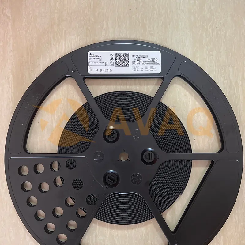
SN65HVD230DR
TI
1000+ $0.403
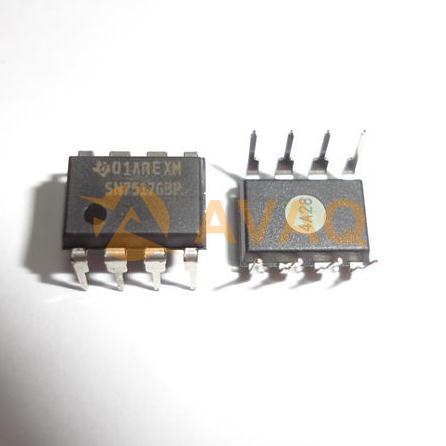
SN75176BP
Texas Instruments
1000+ $0.309

PCF8574AN
TI
8-bit 2.5- to 5.5-V I2C/SMBus I/O expander with interrupt
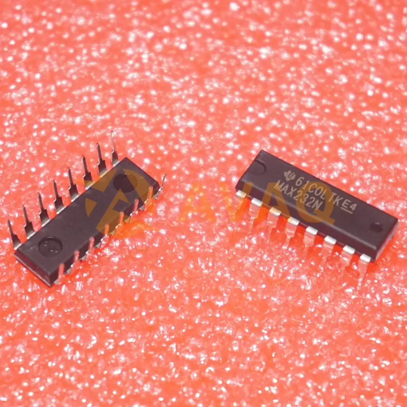
MAX232N
Texas Instruments
Dual Transmitter/Receiver RS-232 16-Pin PDIP Tube
TCA6424RGJR
Texas Instruments, Inc
24-bit translating 1.65- to 5.5-V I2C/SMBus I/O expander with interrupt, reset & config registers
Work well, although I have not attempted to pull 2A from the devices :-)