Payment Method


3.3 V / 5.0 V ECL ÷·2/4, ÷·4/5/6 Divider
Manufacturer:
Mfr.Part #:
MC10EP139DTG
Datasheet:
Case Outline:
9.48
MSL Temp (°C):
260
Container Type:
TUBE
Series:
MC10EP139
EDA/CAD Models:
Please fill in the short form below and we will provide you the quotation immediately.
The MC10/100EP139 is a low skew divide by 2/4, divide by 4/5/6 clock generation chip designed explicitly for low skew clock generation applications. The internal dividers are synchronous to each other, therefore, the common output edges are all precisely aligned. The device can be driven by either a differential or single-ended ECL or, if positive power supplies are used, LVPECL input signals. In addition, by using the VBB output, a sinusoidal source can be AC coupled into the device. If a single-ended input is to be used, the VBB output should be connected to the CLKbar input and bypassed to ground via a 0.01uF capacitor.
The common enable (ENbar) is synchronous so that the internal dividers will only be enabled/disabled when the internal clock is already in the LOW state. This avoids any chance of generating a runt clock pulse on the internal clock when the device is enabled/disabled as can happen with an asynchronous control. The internal enable flip-flop is clocked on the falling edge of the input clock, therefore, all associated specification limits are referenced to the negative edge of the clock input.
Upon startup, the internal flip-flops will attain a random state; therefore, for systems which utilize multiple EP139s, the master reset (MR) input must be asserted to ensure synchronization. For systems which only use one EP139, the MR pin need not be exercised as the internal divider design ensures synchronization between the divide by 2/4 and the divide by 4/5/6 outputs of a single device. All VCC and VEE pins must be externally connected to power supply to guarantee proper operation.
The 100 Series contains temperature compensation.
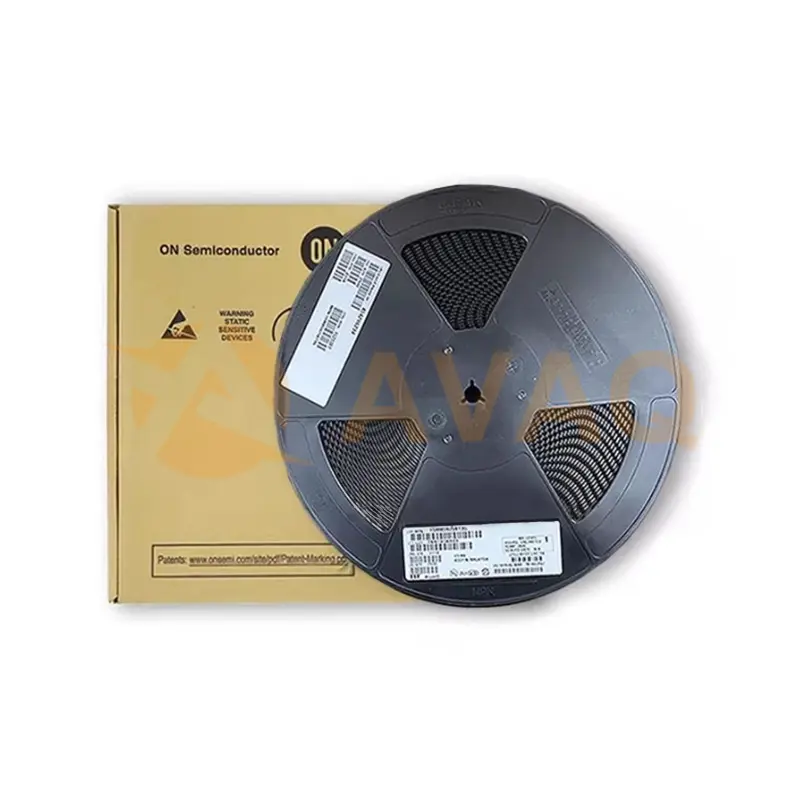


| Status | Active | Case Outline | 9.48 |
| MSL Temp (°C) | 260 | Container Type | TUBE |
| Product Category | Clock Generators & Support Products | Series | MC10EP139 |
| Type | Clock Generators | Maximum Input Frequency | - |
| Max Output Freq | 1 GHz | Number of Outputs | 4 Output |
| Duty Cycle - Max | 50 % | Operating Supply Voltage | 3 V to 5.5 V |
| Operating Supply Current | 84 mA | Minimum Operating Temperature | - 40 C |
| Maximum Operating Temperature | + 85 C | Mounting Style | SMD/SMT |
| Product Type | Clock Generators | Factory Pack Quantity | 75 |
| Subcategory | Clock & Timer ICs | Unit Weight | 0.006737 oz |
After-Sales & Settlement Related
 Payment
Payment Method


For alternative payment channels, please reach out to us at:
[email protected] Shipping & Packing
Shipping Method


AVAQ determines and packages all devices based on electrostatic discharge (ESD) and moisture sensitivity level (MSL) protection requirements.
 Warranty

365-Day Product
Quality Guarantee
We promise to provide 365 days quality assurance service for all our products.
| Qty. | Unit Price | Ext. Price |
|---|---|---|
| 1+ | - | - |
The prices below are for reference only.
All bill of materials (BOM) can be sent via email to ![]() [email protected],
or fill below form to Quote for MC10EP139DTG, guaranteed quotes back within
[email protected],
or fill below form to Quote for MC10EP139DTG, guaranteed quotes back within
![]() 12hr.
12hr.
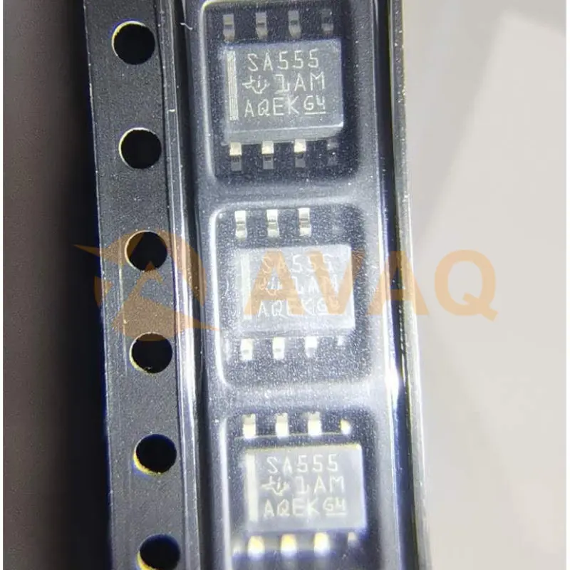
SA555D
ON Semiconductor, LLC
1000+ $0.423
MC14541BCP
ON Semiconductor, LLC
Timers & Support Products LOG CMOS OSILATR TIMER
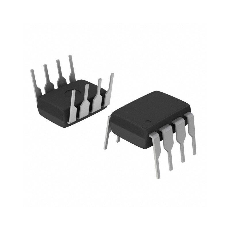
MC1455P1
ON Semiconductor, LLC
Timers & Support Products Timer

KA555
ON Semiconductor, LLC
555 Type, Timer/Oscillator (Single) IC 8-DIP
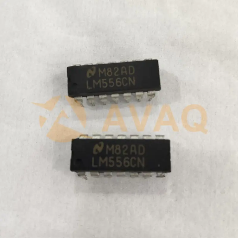
LM556CN
ON Semiconductor, LLC
555 Type, Timer/Oscillator (Dual) IC 14-PDIP