AD8318ACPZ General Description
The AD8318 is a demodulating logarithmic amplifier, capable of accurately converting an RF input signal to a corresponding decibel-scaled output voltage. It employs the progressive compression technique over a cascaded amplifier chain, each stage of which is equipped with a detector cell. The device is used in measurement or controller mode. The AD8318 maintains accurate log conformance for signals of 1 MHz to 6 GHz and provides useful operation to 8 GHz. The input range is typically 60 dB (re: 50 Ω) with error less than ±1 dB. The AD8318 has a 10 ns response time that enables RF burst detection to beyond 45 MHz. The device provides unprecedented logarithmic intercept stability vs. ambient temperature conditions. A 2 mV/°C slope temperature sensor output is also provided for additional system monitoring. A single supply of 5 V is required. Current consumption is typically 68 mA. Power consumption decreases to <1.5 mW when the device is disabled.
The AD8318 can be configured to provide a control voltage to a VGA, such as a power amplifier or a measurement output, from Pin VOUT. Because the output can be used for controller applications, wideband noise is minimal.
In this mode, the setpoint control voltage is applied to VSET. The feedback loop through an RF amplifier is closed via VOUT, the output of which regulates the amplifier output to a magnitude corresponding to VSET. The AD8318 provides 0 V to 4.9 V output capability at the VOUT pin, suitable for controller applications. As a measurement device, Pin VOUT is externally connected to VSET to produce an output voltage, VOUT, which is a decreasing linear-in-dB function of the RF input signal amplitude.
The logarithmic slope is nominally −25 mV/dB but can be adjusted by scaling the feedback voltage from VOUT to the VSET interface. The intercept is 20 dBm (re: 50 Ω, CW input) using the INHI input. These parameters are very stable against supply and temperature variations.
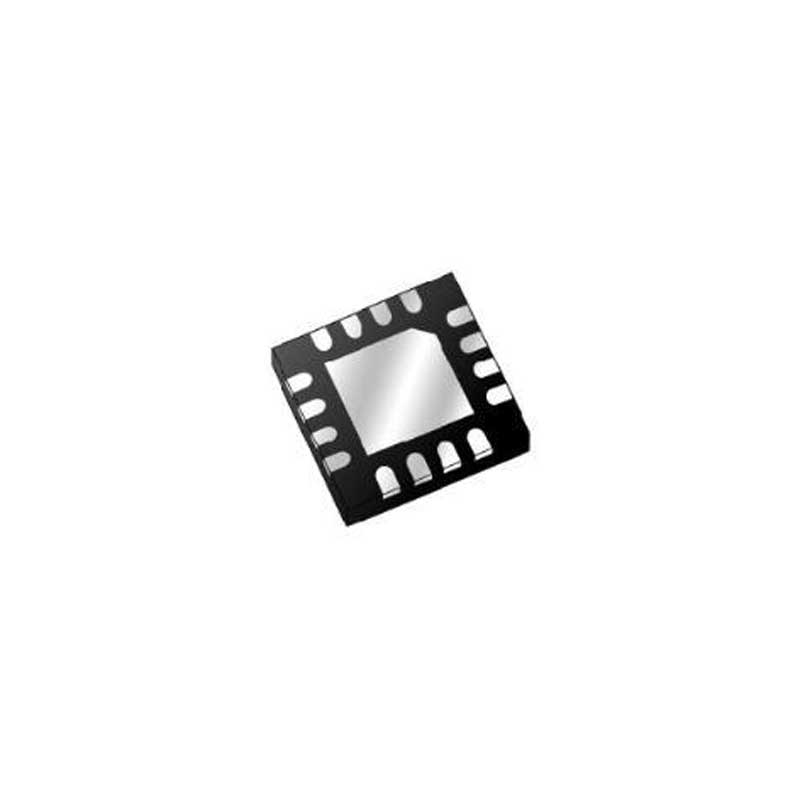
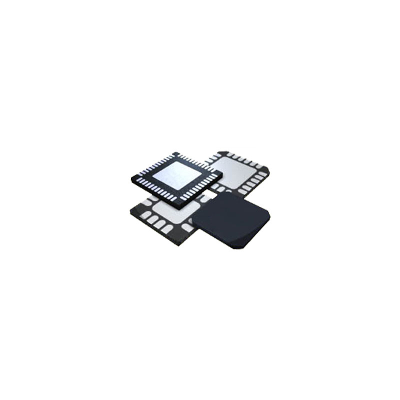
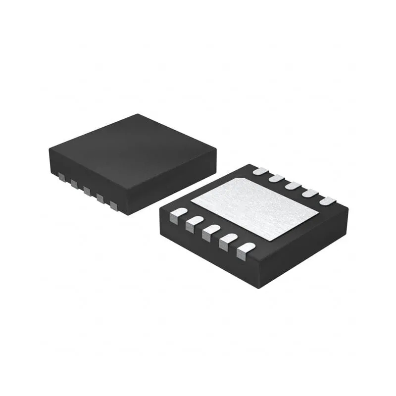
The AD8318 is fabricated on a SiGe bipolar IC process and is available in a 4 mm × 4 mm, 16-lead LFCSP for the operating temperature range of –40°C to +85°C.


 Payment


 Shipping & Packing


 Warranty

Norms. Delivery on time.